Light Sensor Using Wafer-Level Packaging

a technology of light sensor and wafer, applied in the field of semiconductor light sensor, can solve the problems of high power consumption, cost-effective and high-power solutions, and the challenge of cost and power effectiveness in semiconductor techniques, and achieve the effect of cost-effective and reliable solutions

Active Publication Date: 2010-07-29
MAXIM INTEGRATED PROD INC
View PDF62 Cites 69 Cited by
  • Summary
  • Abstract
  • Description
  • Claims
  • Application Information

AI Technical Summary

Benefits of technology

[0007]The present invention provides systems, devices and methods relating to miniature low-power light sensors. With the present invention, a light sensitive component, such as a diode, is fabricated on the front side of a silicon wafer. Connectivity from the front side of the wafer to the back side of the wafer is provided by TSVs. Solder bumps are placed on the back side of the wafer to provide coupling to

Problems solved by technology

However, this approach requires significant semiconductor real estate and fan out resistance, resulting in a costly and high power consuming

Method used


Image

  • Light Sensor Using Wafer-Level Packaging
  • Light Sensor Using Wafer-Level Packaging
  • Light Sensor Using Wafer-Level Packaging

Examples


Embodiment Construction

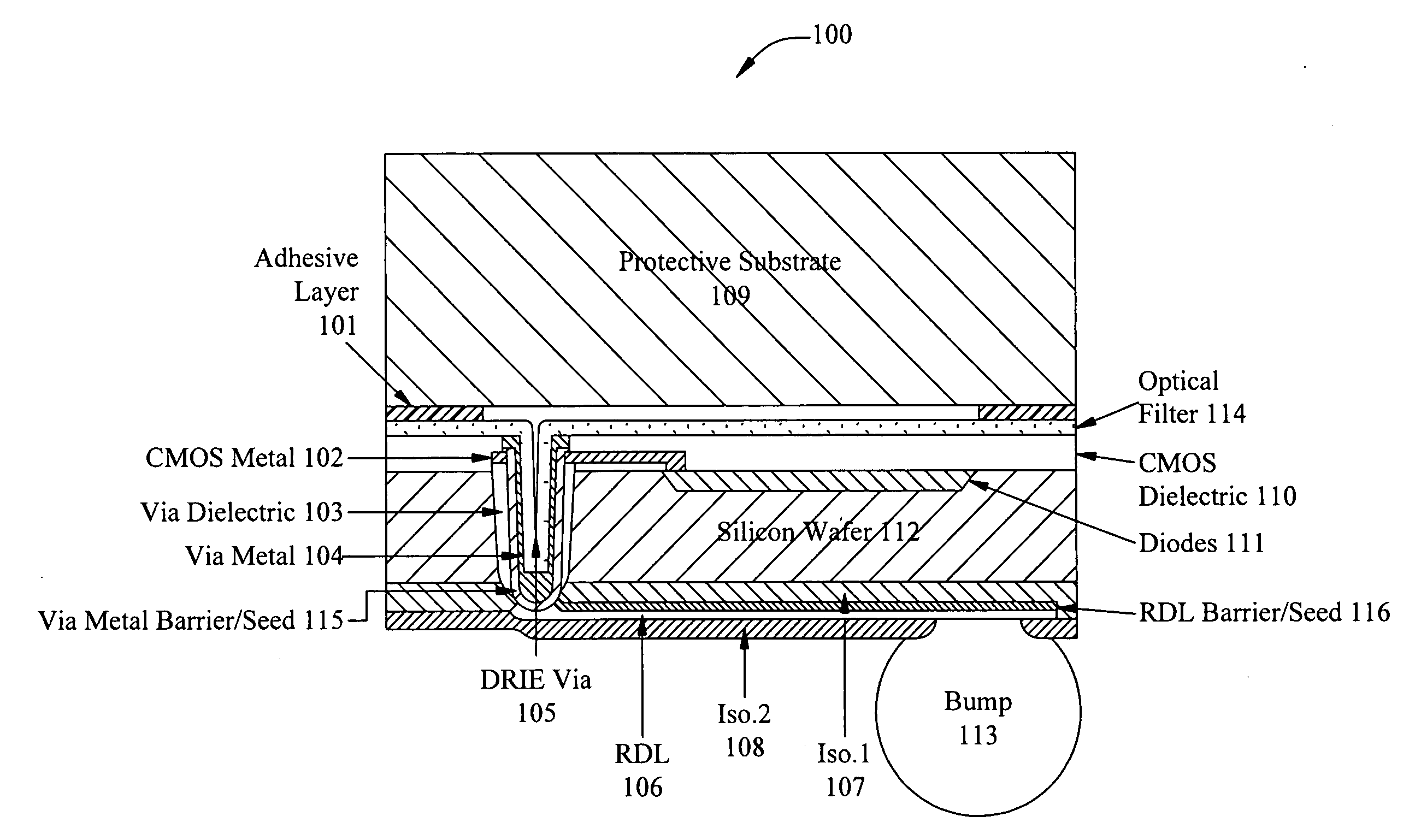
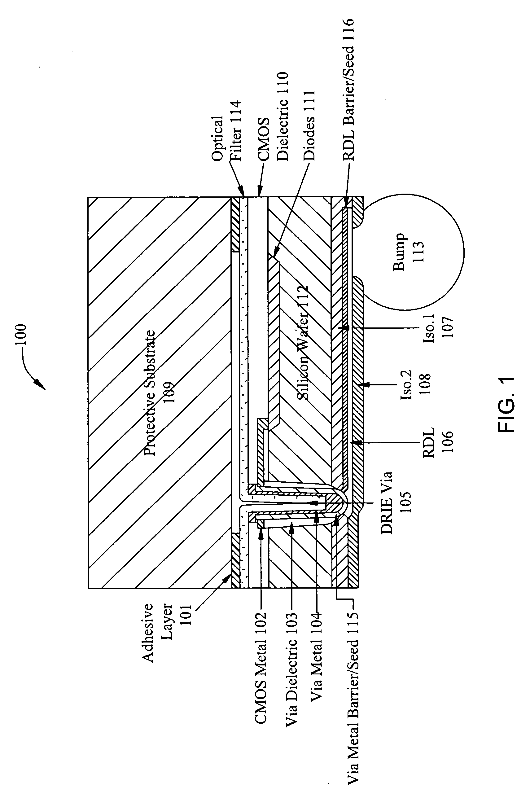
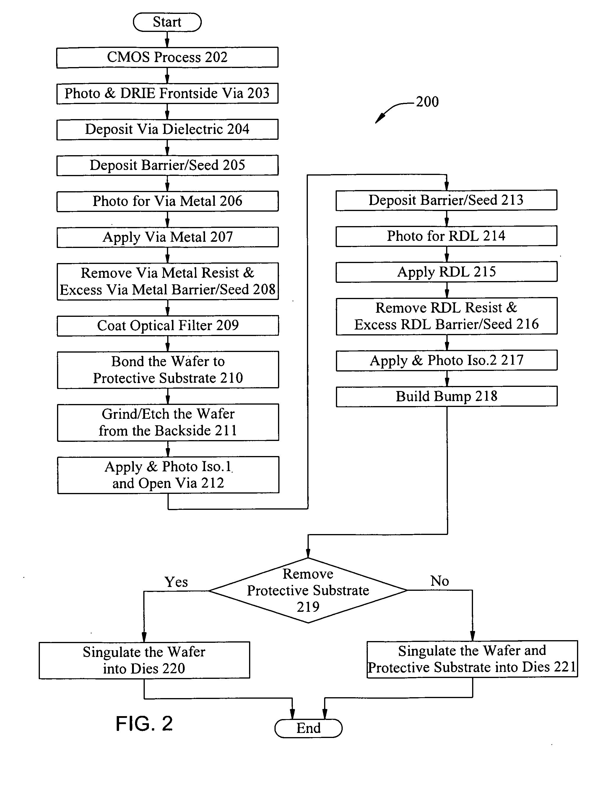
[0019]Embodiments of the present invention provide systems, devices and methods relating to miniature low-power light sensors. The present invention achieves cost and reliability benefits with an efficient integration of Complementary Metal-Oxide-Semiconductor (CMOS) photo diode sensors, the use of TSVs for electrical connectivity, and the selection of solder bumps with certain characteristics. For the electrical connectivity, the invention employs TSVs that connect the light sensitive photo diodes and other devices on the front side to the back side of the die. On the back side of the die, solder bumps are located to facilitate connection with a printed circuit board, or other device. Using specially dimensioned solder bumps for wafer bumping eliminates the need for underfill, e.g. filling of the space between the chip and the PCB, and results in a cost-effective and reliable solution. Additionally, in order to ensure optical access to the sensor, the present invention employs an o...


PUM


Abstract

The present invention provides systems, devices and methods for fabricating miniature low-power light sensors. With the present invention, a light sensitive component, such as a diode, is fabricated on the front side of a silicon wafer. Connectivity from the front side of the wafer to the back side of the wafer is provided by a through silicon via. Solder bumps are then placed on the back side of the wafer to provide coupling to a printed circuit board. The techniques described in the present invention may also be applied to other types of semiconductor devices, such as light-emitting diodes, image sensors, pressure sensors, and flow sensors.

Description

BACKGROUND[0001]A. Technical Field[0002]The present invention relates generally to semiconductor light sensors, and more particularly to using various semiconductor fabrication and wafer level packaging techniques for fabricating miniature low power light sensors.[0003]B. Background of the Invention[0004]Light sensors are ubiquitous in modern society. Some applications use reflected light with optical detection for position sensing; these applications include bar code readers, laser printers and auto focusing microscopes. Other applications, such as digital cameras, cell phones and laptops, use optical sensors to gauge the amount of ambient light, and minimize the device's power consumption by regulating the intensity of the screen light as a function of the amount of the ambient light. Further, ambient-light sensors are integrated in laptops to adjust the screen's backlight to comfortable levels for the viewer. Light sensors may also be used in industrial applications.[0005]Light s...

Claims


Application Information

Patent Timeline
IPC IPC(8): H01L33/00H01L31/0232H01L29/84H01L31/02H01L29/66
CPCH01L27/144H01L31/18H01L31/101H01L2224/13H01L2224/05569H01L2224/05008H01L2224/05548H01L2224/05001H01L2224/051H01L2224/056H01L23/481H01L24/11H01L24/13H01L24/02H01L2924/0001H01L2224/02372H01L2224/0231H01L2224/131H01L2224/13024H01L24/05
Inventor SAMOILOV, ARKADII V.BERGEMONT, ALBERTLO, CHIUNG-C.HOLENARSIPUR, PRASHANTHLONG, JAMES PATRICK
Owner MAXIM INTEGRATED PROD INC
Why Eureka
Try Eureka