Semiconductor memory device including a cylinder type storage node and a method of fabricating the same

a memory device and cylinder technology, applied in semiconductor devices, electrical devices, capacitors, etc., can solve the problems of limited structural instability and twin bit errors or multi-bit errors, so as to achieve the critical dimension (cd) of the storage node and the electrical properties required, the effect of sufficient mechanical stability of cylinder type storage nodes

a memory device and cylinder technology, applied in semiconductor devices, electrical devices, capacitors, etc., can solve the problems of limited structural instability and twin bit errors or multi-bit errors, so as to achieve the critical dimension (cd) of the storage node and the electrical properties required, the effect of sufficient mechanical stability of cylinder type storage nodes

US20100187588A1Inactive Publication Date: 2010-07-29SAMSUNG ELECTRONICS CO LTD

Image

  • Semiconductor memory device including a cylinder type storage node and a method of fabricating the same
  • Semiconductor memory device including a cylinder type storage node and a method of fabricating the same
  • Semiconductor memory device including a cylinder type storage node and a method of fabricating the same

Examples


Embodiment Construction

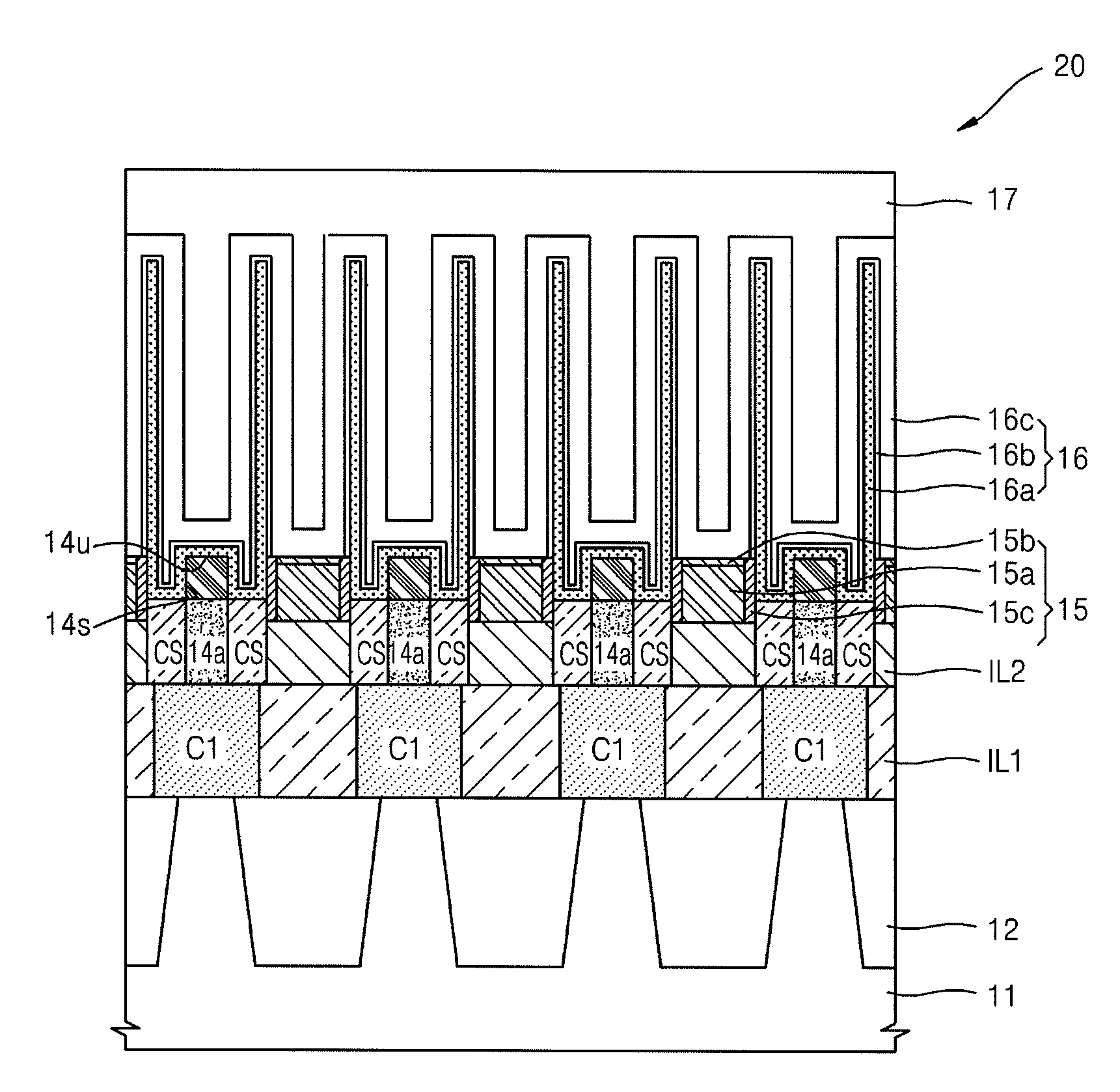
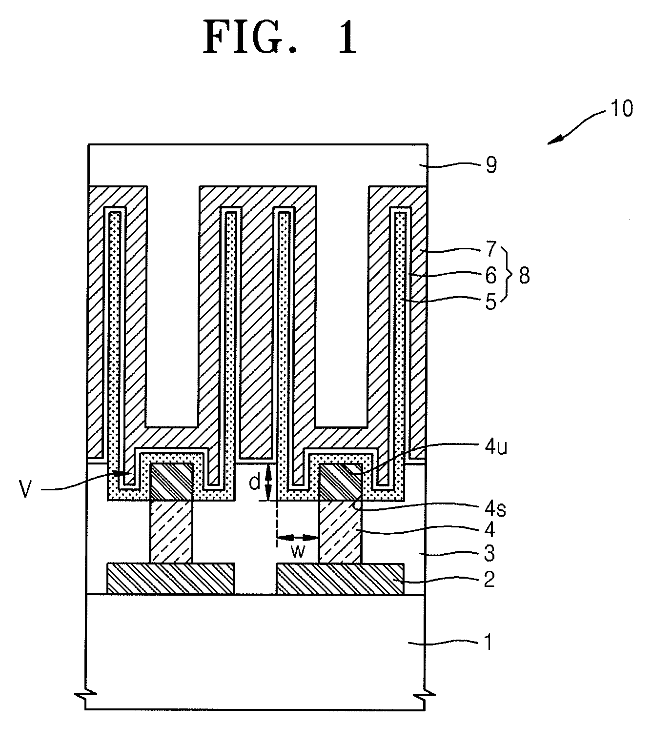
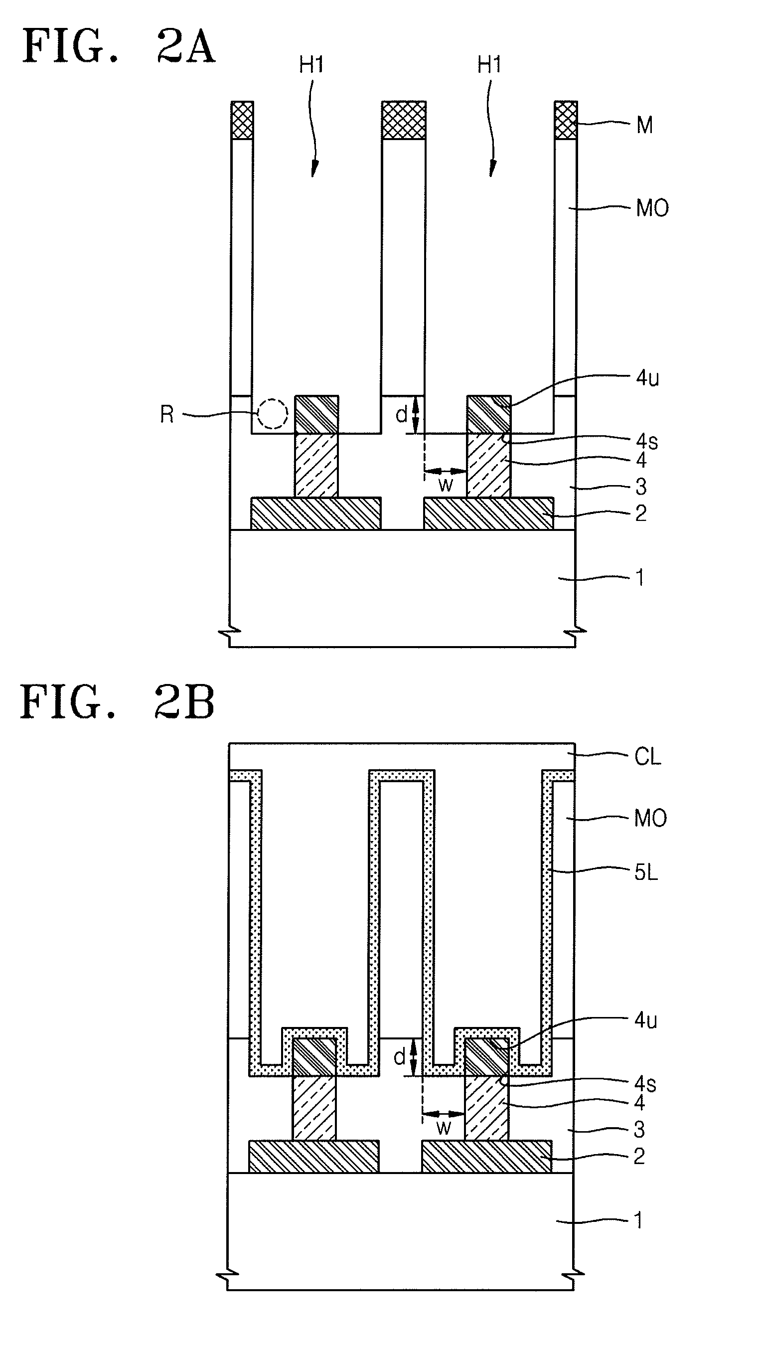
[0025]Exemplary embodiments of the present invention will be described with reference to accompanying drawings.

[0026]The example embodiments will now be described more fully with reference to the accompanying drawings. The invention may, however, be embodied in many different forms and should not be construed as being limited to the exemplary embodiments set forth herein. Like reference numerals refer to like elements.

[0027]It will be understood that when an element is referred to as being “on” another element, it can be directly on the other element or intervening elements may be present there between. In contrast, when an element is referred to as being “directly on” another element, there are no intervening elements present. As used herein, the term “and / or” includes any and all combinations of one or more of the associated listed items.

[0028]The terminology used herein is for the purpose of describing particular embodiments only and is not intended to be limiting of the inventio...


PUM


Abstract

Provided is a semiconductor memory device including cylinder type storage nodes and a method of fabricating the semiconductor memory device. The semiconductor memory device includes: a semiconductor substrate including switching devices; a recessed insulating layer including storage contact plugs therein, wherein the storage contact plugs are electrically connected to the switching devices and the recessed insulating layer exposes at least some portions of upper surfaces and side surfaces of the storage contact plugs. The semiconductor device further includes cylinder type storage nodes each having a lower electrode. The lower electrode contacting the at least some portions of the exposed upper surfaces and side surfaces of the storage node contact plugs.

Description

CROSS-REFERENCE TO RELATED APPLICATIONS[0001]This application claims priority to Korean Patent Application No. 10-2009-0006979, filed on Jan. 29, 2009, the disclosure of which is hereby incorporated by reference herein in its entirety.BACKGROUND[0002](i) Technical Field[0003]The present disclosure relates to a semiconductor memory device and to a method of fabricating the same, and more particularly, to a semiconductor memory device including a cylinder type storage node and to a method of fabricating the semiconductor memory device.[0004](ii) Description of the Related Art[0005]A memory cell of a direct random access memory (DRAM) among semiconductor memory devices may include a field effect transistor as a switching device for controlling read / write operations, and a capacitor for storing information. As the scale of the DRAM has been reduced, the area occupied by the capacitor of the memory cell has been continuously decreased. To ensure a sufficient effective capacity despite th...

Claims


Application Information

Patent Timeline
29 Jul 2010
Publication
US20100187588A1
IPC
H01L27/108
CPC
H01L27/10817; H01L28/91; H01L27/10852; H10B12/318; H10B12/033; H10B99/00; H10B12/00
Inventors
KIM, GIL-SUB; PARK, WON MO