Through-Silicon Via Sidewall Isolation Structure

a technology of throughsilicon via and isolation structure, which is applied in the direction of semiconductor devices, semiconductor/solid-state device details, electrical devices, etc., can solve the problem of thin layer on the surface of the substra

Inactive Publication Date: 2010-07-29
TAIWAN SEMICON MFG CO LTD
View PDF8 Cites 213 Cited by
  • Summary
  • Abstract
  • Description
  • Claims
  • Application Information

AI Technical Summary

Benefits of technology

[0008]These and other problems are generally solved or circumvented, and technical advantages are generally achieved, by embodiments of the present invention which provide a semiconductor device having an improved through-silicon via with a sidewall isolation structure.
[0009]In accordance with an embodiment of the present invention, a semiconductor device comprising a substrate having electrical circuitry formed thereon is provided. One or more dielectric layers are formed over the substrate, and an opening extending through the one or more dielectric layers into the substrate is formed. The opening is filled with a conductive material, and a low-K dielectric layer is interposed between the substrate and the conductive material.
[0010]In accordance with another embodiment of the present invention, a method for creating a semiconductor device is provided. The method comprises providing a substrate, and forming an opening in the substrate extending from a first

Problems solved by technology

However, the barrier layer formation processes have difficulty in forming a thin layer along the sidewalls of the via formed in the substrate and often result in a thick layer on the s

Method used


Image

  • Through-Silicon Via Sidewall Isolation Structure
  • Through-Silicon Via Sidewall Isolation Structure
  • Through-Silicon Via Sidewall Isolation Structure

Examples


Embodiment Construction

[0014]The making and using of the presently preferred embodiments are discussed in detail below. It should be appreciated, however, that the present invention provides many applicable inventive concepts that can be embodied in a wide variety of specific contexts. The specific embodiments discussed are merely illustrative of specific ways to make and use the invention, and do not limit the scope of the invention.

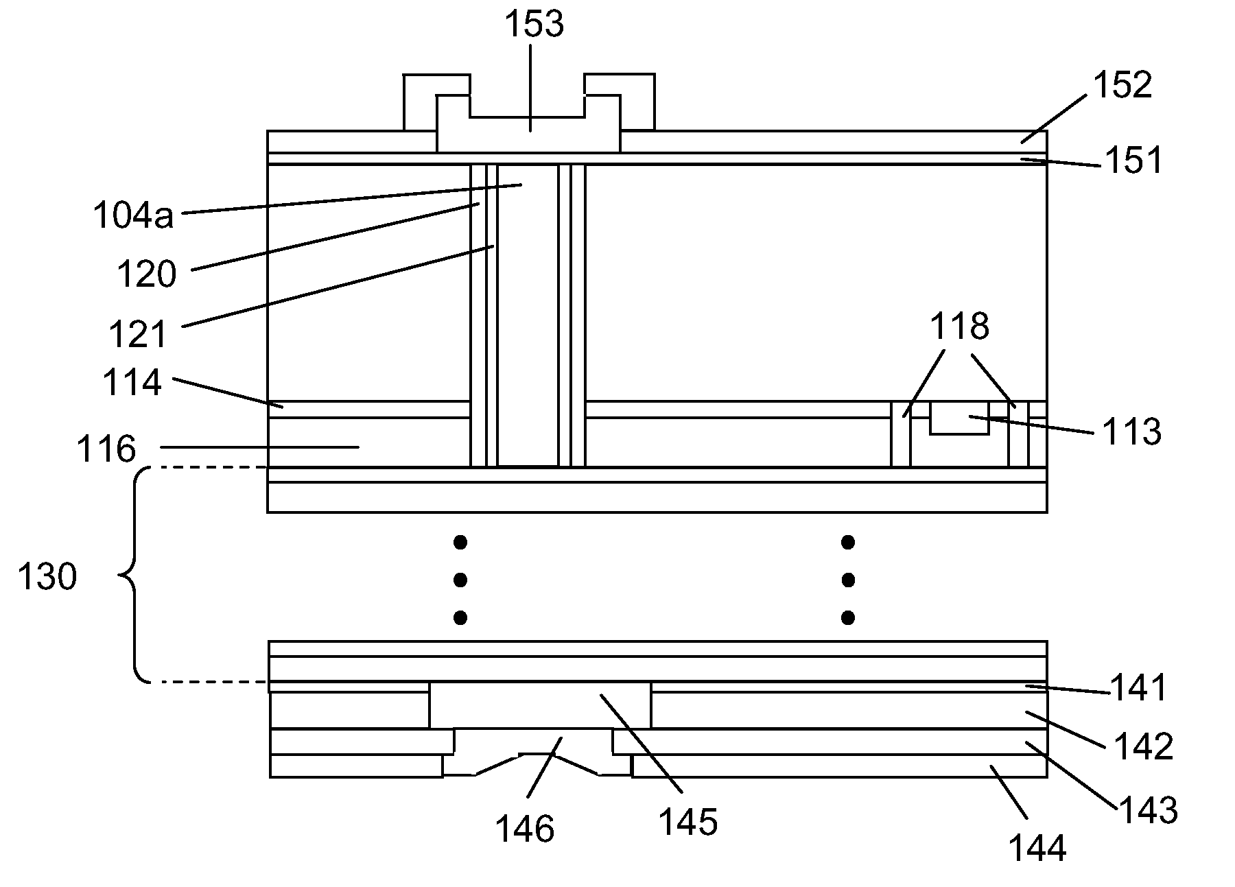
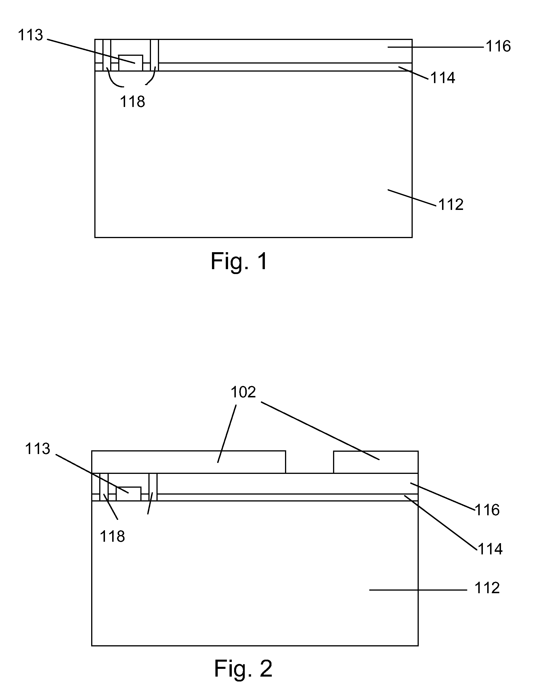
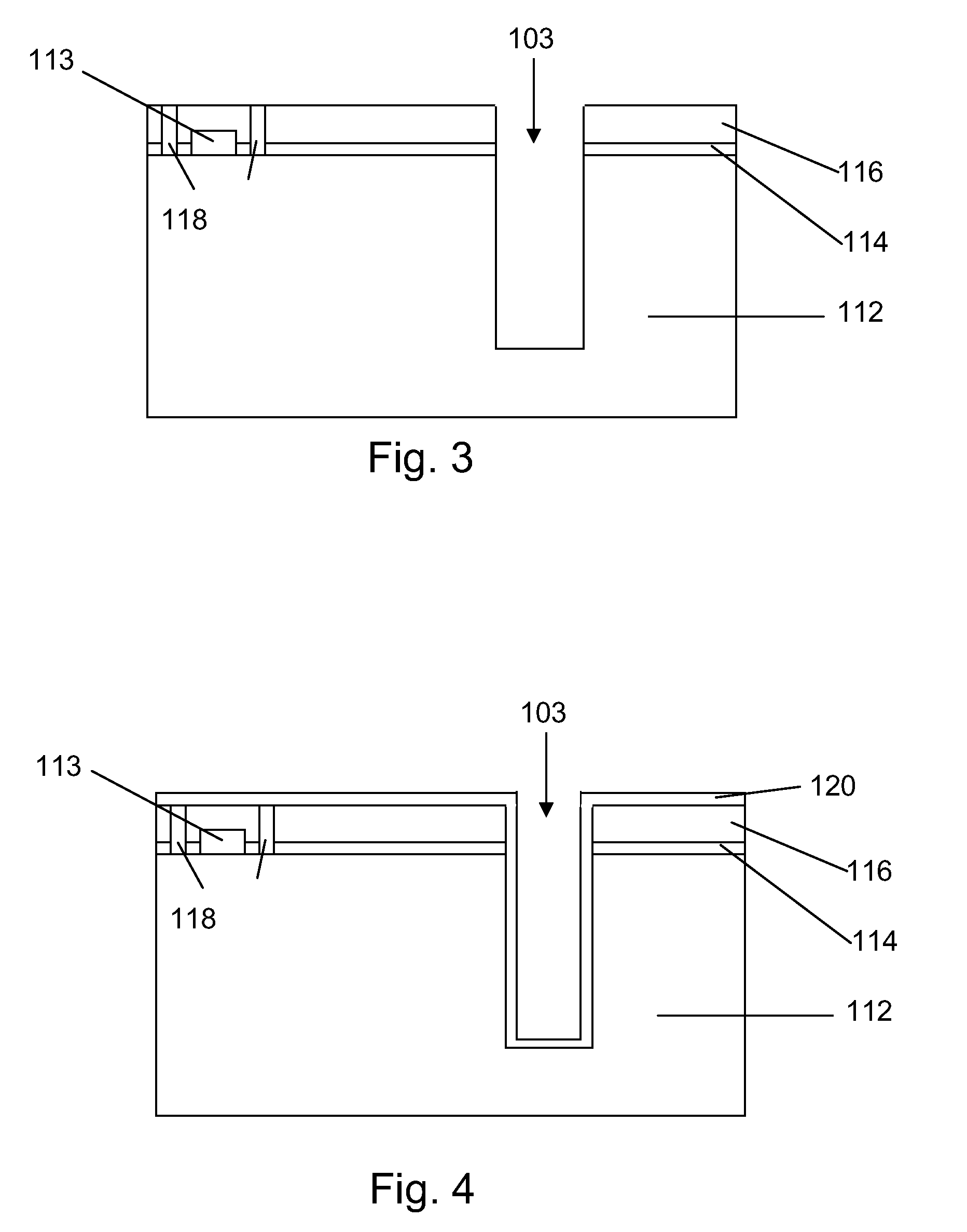
[0015]FIGS. 1-8 are cross-sectional views of intermediate stages in the making of an embodiment of the present invention. Referring first to FIG. 1, a substrate 112 is shown having electrical circuitry 113 formed thereon. The substrate 112 may comprise, for example, bulk silicon, doped or undoped, or an active layer of a semiconductor-on-insulator (SOI) substrate. Generally, an SOI substrate comprises a layer of a semiconductor material, such as silicon, formed on an insulator layer. The insulator layer may be, for example, a buried oxide (BOX) layer or a silicon oxide layer....


PUM


Abstract

A system and method for an improved through-silicon via isolation structure is provided. An embodiment comprises a semiconductor device having a substrate with electrical circuitry formed thereon. One or more dielectric layers are formed over the substrate, and an opening is etched into the structure extending from a surface of the one or more dielectric layers through the one or more dielectric layers into the substrate; the opening having sidewalls. A low-K dielectric layer is formed over the sidewalls of the opening. The opening is filled with a conductive material and/or a barrier layer creating a through-silicon via that is isolated from the surrounding substrate by the low-K dielectric layer.

Description

[0001]This application claims the benefit of U.S. Provisional Application No. 61 / 147,871, filed on Jan. 28, 2009, entitled “Through-Silicon Via Sidewall Isolation Structure,” which application is hereby incorporated herein by reference.TECHNICAL FIELD[0002]The present invention relates generally to a system and method for improved through-silicon vias and, more particularly, to a system and method for a through-silicon via sidewall isolation structure.BACKGROUND[0003]Since the invention of the integrated circuit (IC), the semiconductor industry has experienced rapid growth due to continuous improvements in the integration density of various electronic components (e.g., transistors, diodes, resistors, capacitors, etc.). For the most part, this improvement in integration density has come from repeated reductions in minimum feature size, which allows more components to be integrated into a given area.[0004]In an attempt to further increase circuit density, three-dimensional (3D) ICs ha...

Claims


Application Information

Patent Timeline
IPC IPC(8): H01L23/48H01L21/768
CPCH01L21/76898H01L23/5329H01L24/05H01L24/06H01L2224/0557H01L2924/04941H01L2924/14H01L2924/0002H01L2924/19041H01L2924/19043H01L2924/30105H01L2924/01019H01L2224/05552
Inventor YU, CHEN-HUACHIOU, WEN-CHIHWU, WENG-JIN
Owner TAIWAN SEMICON MFG CO LTD
Why Eureka
Try Eureka