

Magnetoresistive element and thin-film magnetic head
- Summary
- Abstract
- Description
- Claims
- Application Information
AI Technical Summary
Benefits of technology
Problems solved by technology
Method used
Image

Examples
first embodiment
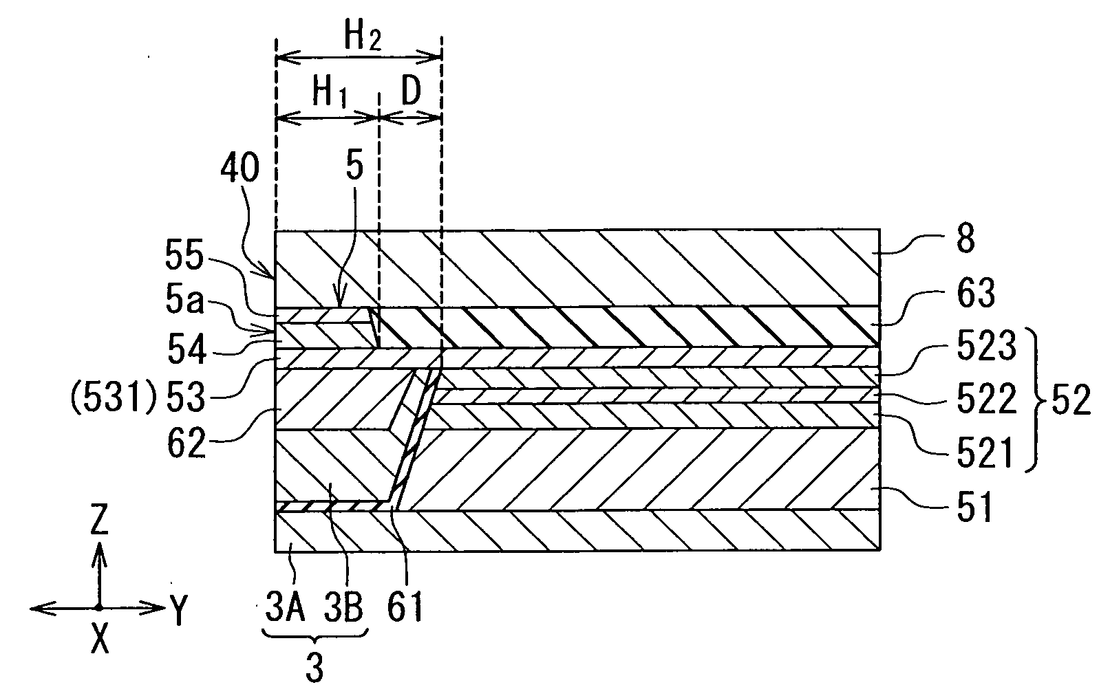
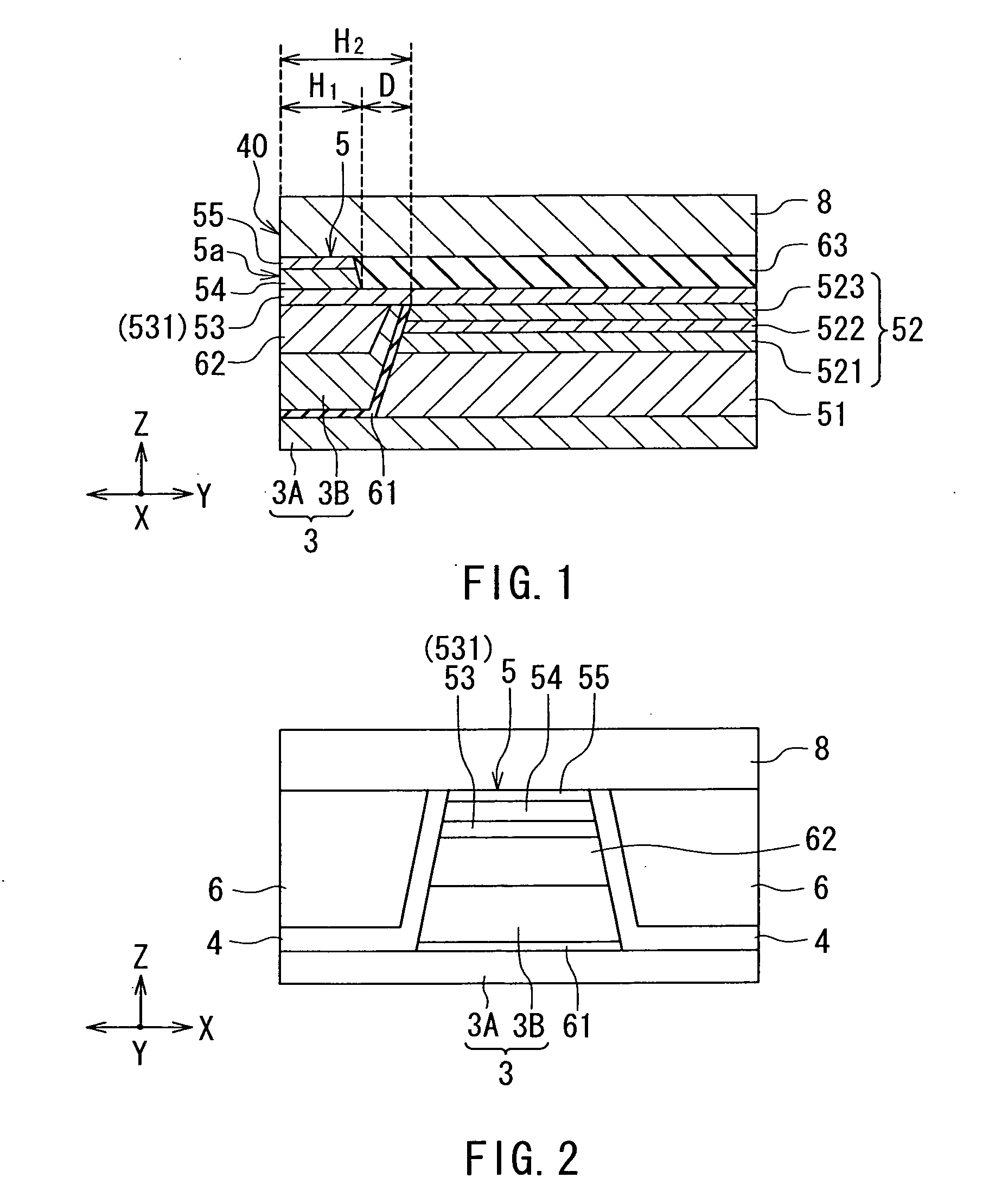
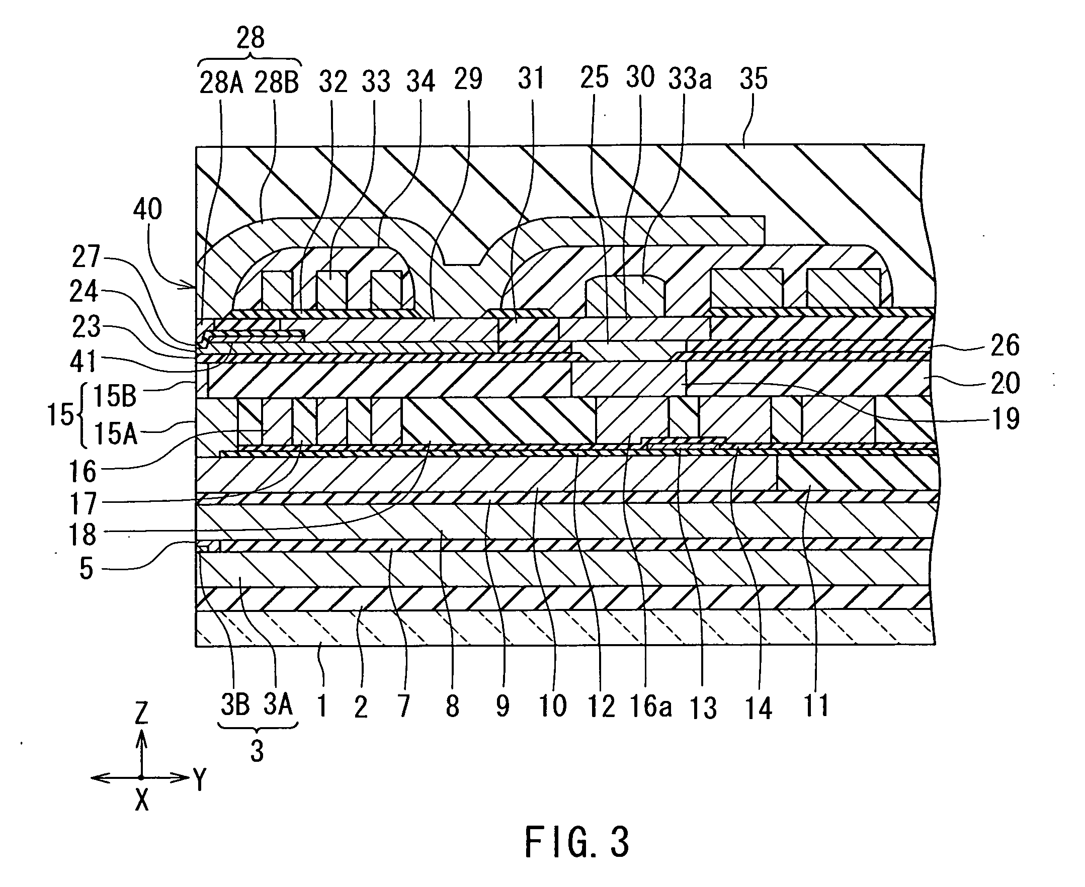
[0055]Embodiments of the present invention will now be described in detail with reference to the drawings. Reference is first made to FIG. 5 to describe a slider 210 including a thin-film magnetic head according to a first embodiment of the present invention. In a magnetic disk drive the slider 210 is placed to face toward a circular-plate-shaped recording medium (a magnetic disk) that is driven to rotate. In FIG. 5 the X direction is across the tracks of the recording medium, the Y direction is perpendicular to the surface of the recording medium, and the Z direction is the direction of travel of the recording medium as seen from the slider 210. The X, Y and Z directions are orthogonal to one another. The slider 210 has a base body 211. The base body 211 is nearly hexahedron-shaped. One of the six surfaces of the base body 211 is designed to face toward the surface of the recording medium. At this one of the six surfaces, there is formed a medium facing surface 40 to face toward th...
second embodiment
[0132]A second embodiment of the present invention will now be described with reference to FIG. 20 and FIG. 21. FIG. 20 is a cross-sectional view of a read head including an MR element according to the second embodiment. FIG. 21 is a front view of the read head shown in FIG. 20. The coupling portion 53 of the MR element 5 according to the second embodiment includes: a nonmagnetic conductive layer 531 disposed on the flattened top surfaces of the pinned layer 52, the insulating film 61, the second layer 3B and the nonmagnetic conductive layer 62; and a tunnel barrier layer 532 disposed on the nonmagnetic conductive layer 531. The configuration and function of the nonmagnetic conductive layer 531 are the same as those of the first embodiment. The tunnel barrier layer 532 is disposed between the nonmagnetic conductive layer 531 and the free layer 54. The tunnel barrier layer 532 is made of an insulating material such as alumina, SiO2 or MgO.
[0133]In a method of fabricating the read hea...
third embodiment
[0136]A third embodiment of the present invention will now be described with reference to FIG. 22 and FIG. 23. FIG. 22 is a cross-sectional view of a read head including an MR element according to the third embodiment. FIG. 23 is a front view of the read head shown in FIG. 22. The coupling portion 53 of the MR element 5 according to the third embodiment includes: a tunnel barrier layer 532 disposed on the flattened top surfaces of the pinned layer 52, the insulating film 61, the second layer 3B and the nonmagnetic conductive layer 62; and a nonmagnetic conductive layer 531 disposed on the tunnel barrier layer 532. The configuration and function of the nonmagnetic conductive layer 531 are the same as those of the first embodiment. The tunnel barrier layer 532 is disposed between the nonmagnetic conductive layer 531 and the pinned layer 52. The tunnel barrier layer 532 is made of an insulating material such as alumina, SiO2 or MgO.
[0137]In a method of fabricating the read head accordi...
PUM
 Abstract
Description
Claims
Application Information