
Use of a biased precoat for reduced first wafer defects in high-density plasma process

a plasma process and biased technology, applied in the field of chemical vapor deposition processes, to achieve the effect of reducing first wafer defects and minimizing yield losses

Active Publication Date: 2010-07-29
TEXAS INSTR INC
View PDF1 Cites 195 Cited by
  • Summary
  • Abstract
  • Description
  • Claims
  • Application Information

AI Technical Summary

Benefits of technology

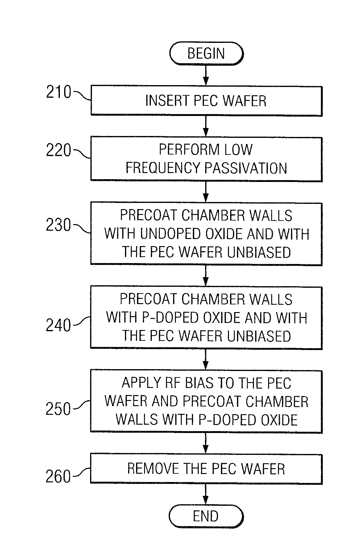
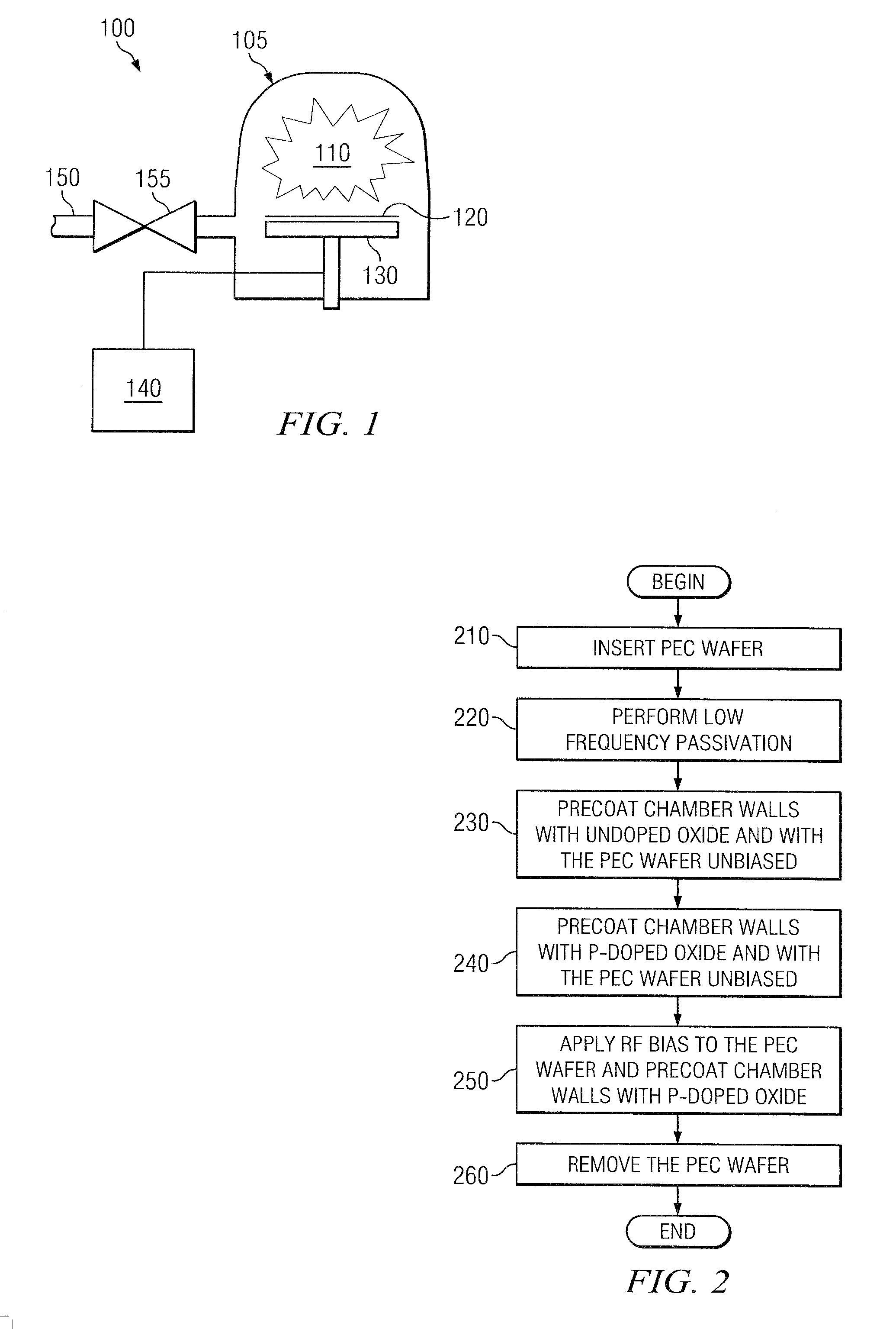
[0007]Furthermore, the application of HF RF power that biases the PEC wafer also produces gas flow patterns in the deposition chamber during precoat that are similar to the gas flow patterns during a subsequent film deposition on silicon wafers, which causes loose particles in the deposition chamber to fall on the PEC wafer during precoat instead of on the silicon wafers and in particular the first silicon wafer during film deposition subsequent to the cleaning and precoat processes. If the loose particles fall on the silicon wafers during film deposition, the loose particles would become embedded in the deposited film and cause rip-outs during chemical-mechanical polishing (CMP). By applying HF RF power that biases the PEC wafer during precoat, the loose particles fall on the PEC wafer instead of the silicon wafers, thereby minimizing yield losses caused by embedded loose particles.
[0008]According to various embodiments, the present teachings include a method for reducing first wafer defects that can include inserting a protective cover and applying power to bias the protective cover while simultaneously precoating the deposition chamber.

Problems solved by technology

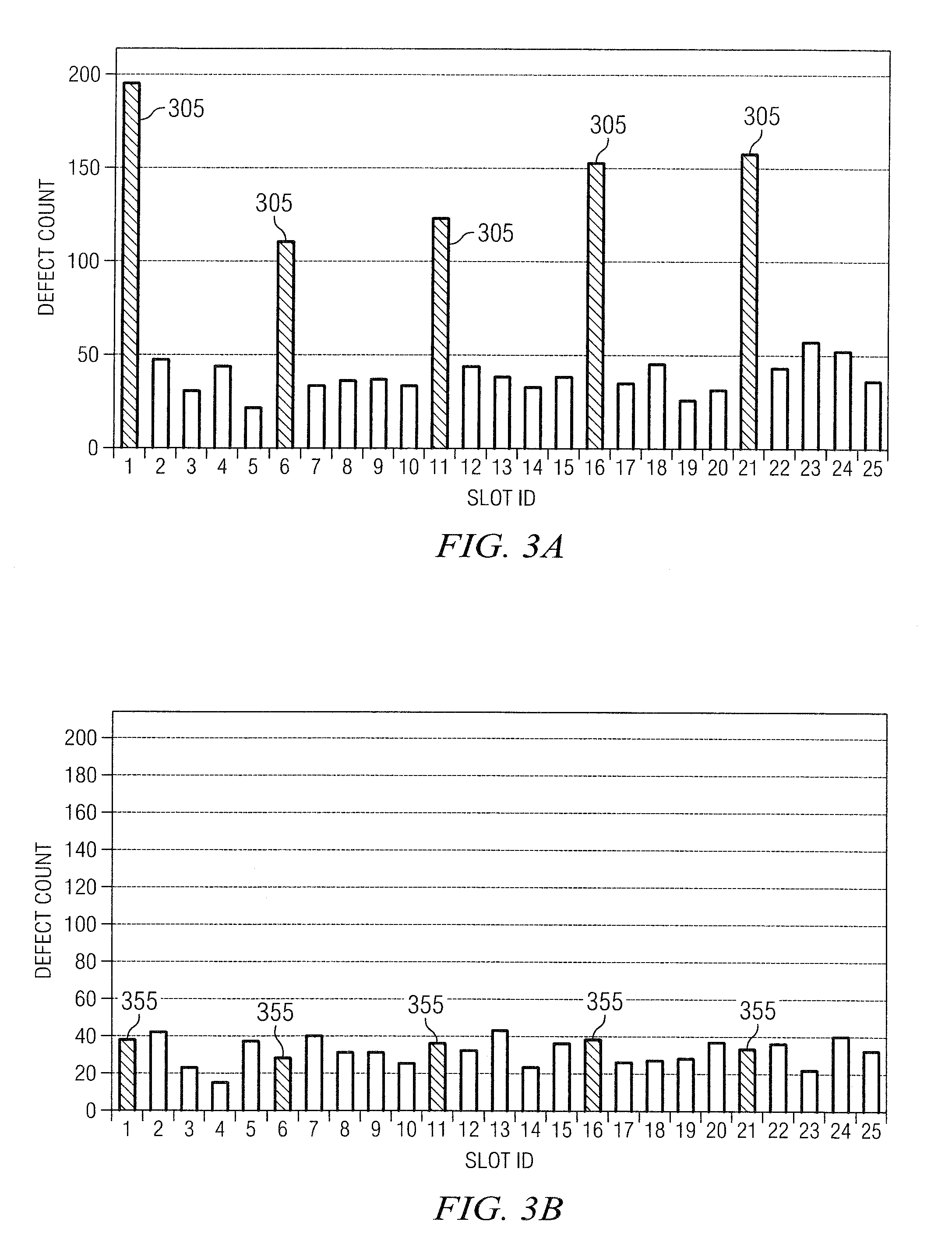
If the loose particles fall on the silicon wafers during film deposition, the loose particles would become embedded in the deposited film and cause rip-outs during chemical-mechanical polishing (CMP).

Method used


Image

  • Use of a biased precoat for reduced first wafer defects in high-density plasma process
  • Use of a biased precoat for reduced first wafer defects in high-density plasma process
  • Use of a biased precoat for reduced first wafer defects in high-density plasma process

Examples


Embodiment Construction

[0016]Reference will now be made in detail to exemplary embodiments of the invention, examples of which are illustrated in the accompanying drawings. Wherever possible, the same reference numbers will be used throughout the drawings to refer to the same or like parts.

[0017]Notwithstanding that the numerical ranges and parameters setting forth the broad scope of the invention are approximations, the numerical values set forth in the specific examples are reported as precisely as possible. Any numerical value, however, inherently contains certain errors necessarily resulting from the standard deviation found in their respective testing measurements. Moreover, all ranges disclosed herein are to be understood to encompass any and all sub-ranges subsumed therein. For example, a range of “less than 10” can include any and all sub-ranges between (and including) the minimum value of zero and the maximum value of 10, that is, any and all sub-ranges having a minimum value of equal to or great...


PUM

PropertyMeasurementUnit
Fractionaaaaaaaaaa
Fractionaaaaaaaaaa
Poweraaaaaaaaaa

Abstract

According to various embodiments, the present teachings include methods for reducing first wafer defects in a high-density plasma chemical vapor deposition process. In an exemplary embodiment, the method can include running a deposition chamber for deposition of film on a first batch of silicon wafers and then cleaning interior surfaces of the deposition chamber. The method can further include inserting a protective electrostatic chuck cover (PEC) wafer on an electrostatic chuck in the deposition chamber and applying power to bias the PEC wafer while simultaneously precoating the deposition chamber with an oxide. The exemplary method can also include re-starting the deposition chamber for deposition of film on a second batch of silicon wafers.

Description

FIELD OF THE INVENTION [0001]The subject matter of this invention relates to chemical vapor deposition processes. More particularly, the subject matter of this invention relates to the use of a biased precoat process for reducing first wafer defects in high-density plasma chemical vapor deposition processes.DESCRIPTION OF THE RELATED ART [0002]High-density plasma (HDP) chemical vapor deposition (CVD) chambers, such as HDP SPEED™ Chamber manufactured by Novellus Systems, are employed to perform HDP CVD: processes to deposit films on a substrate in the fabrication of integrated circuits. Existing HDP CVD processes typically perform film deposition with a processing gas mixture that includes oxygen, silane, and inert gases, such as helium, to achieve simultaneous dielectric etching and deposition. During film deposition, RF power is applied to an electrostatic chuck to bias a silicon wafer placed thereon. Some of the gas molecules are ionized in the plasma and accelerate toward the sur...

Claims


Application Information

Patent Timeline
IPC IPC(8): H01L21/31B05D3/06
CPCC23C16/4404H01L21/31604C23C16/505H01L21/02274
Inventor JAISWAL, RAJNEESH
Owner TEXAS INSTR INC
Learn More