Infrared sensors, focal plane arrays and thermal imaging systems

a technology of infrared sensors and thermal imaging systems, applied in the direction of optical radiation measurement, instruments, material analysis, etc., can solve the problems of difficult control of manufacturing process, difficult to make and expensive, and complicated readout optical setup

Active Publication Date: 2010-08-05
SHANGHAI JUGE ELECTRONICS TECH
View PDF5 Cites 24 Cited by
  • Summary
  • Abstract
  • Description
  • Claims
  • Application Information

AI Technical Summary

Problems solved by technology

Traditional infrared sensors are fabricated using narrow band gap semiconductors or microbolometers, and they are difficult to make and expensive.
This method measures the deflection of the visible lights, and involves complicated readout optical setup.
Its manufacturing process is also difficult to control.
The technology uses optical crystal which is difficult for production.
The optical setup is also complicated, and the detected infrared light is from active infrared illumination, not infrared light emitted from objects.
The suspending reflecting layer is just a reflective film structure and has low thermal capacity.

Method used


Image

  • Infrared sensors, focal plane arrays and thermal imaging systems
  • Infrared sensors, focal plane arrays and thermal imaging systems
  • Infrared sensors, focal plane arrays and thermal imaging systems

Examples


Embodiment Construction

[0050]Various embodiments of the invention will be described in accordance with the following drawings.

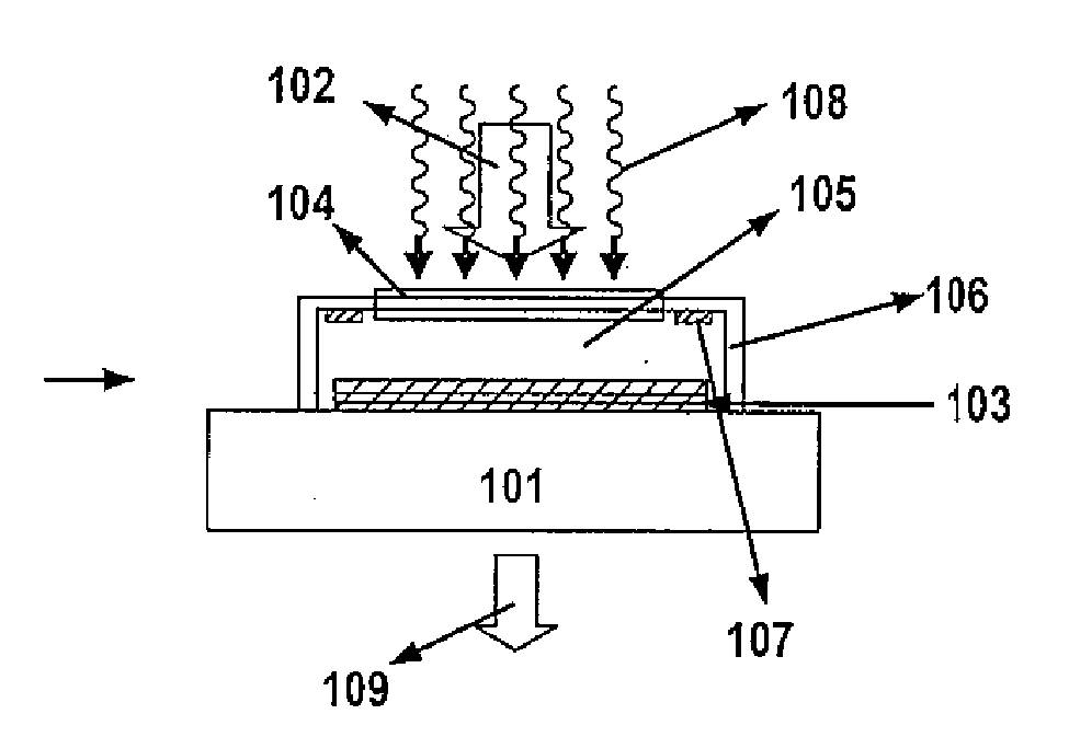
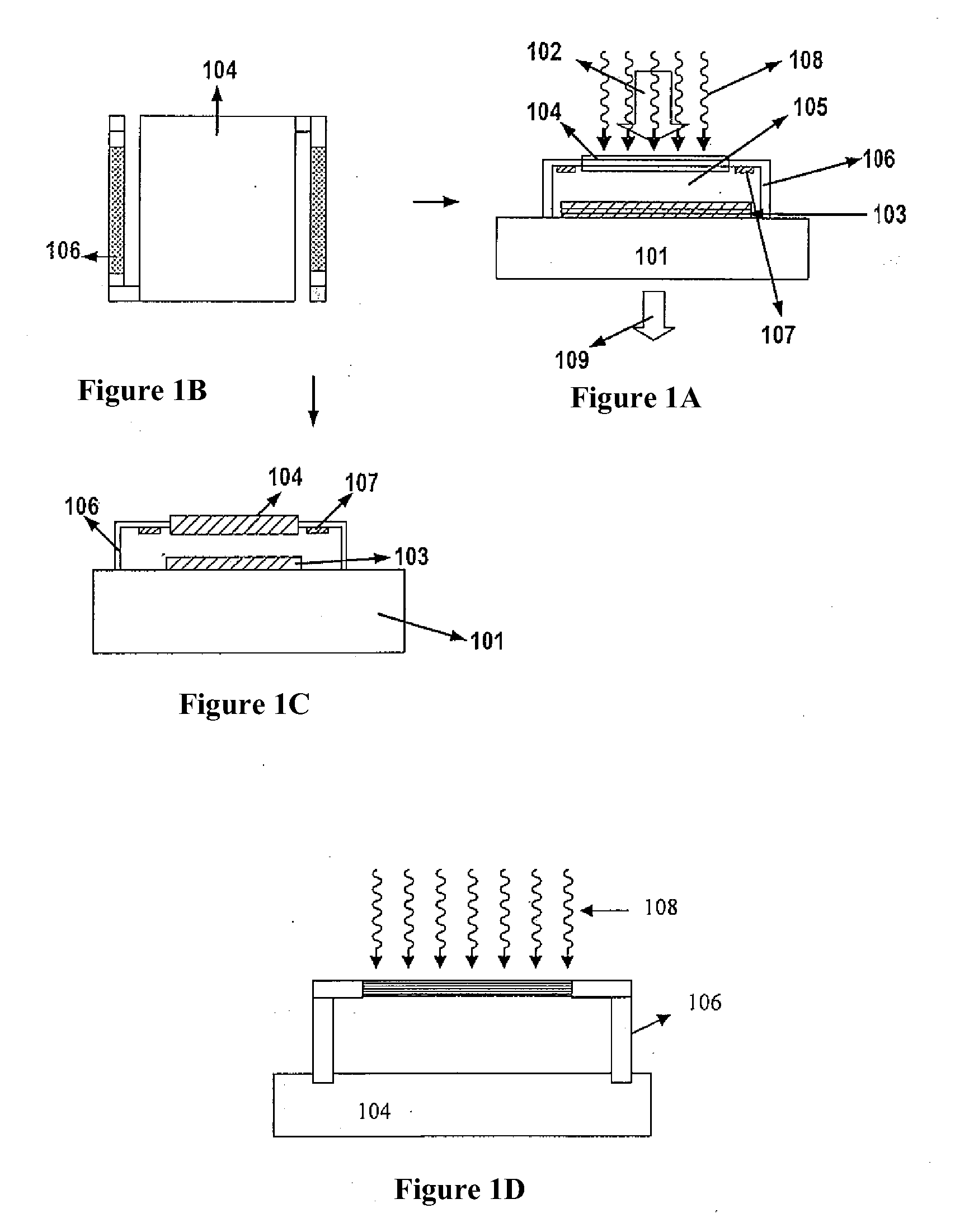
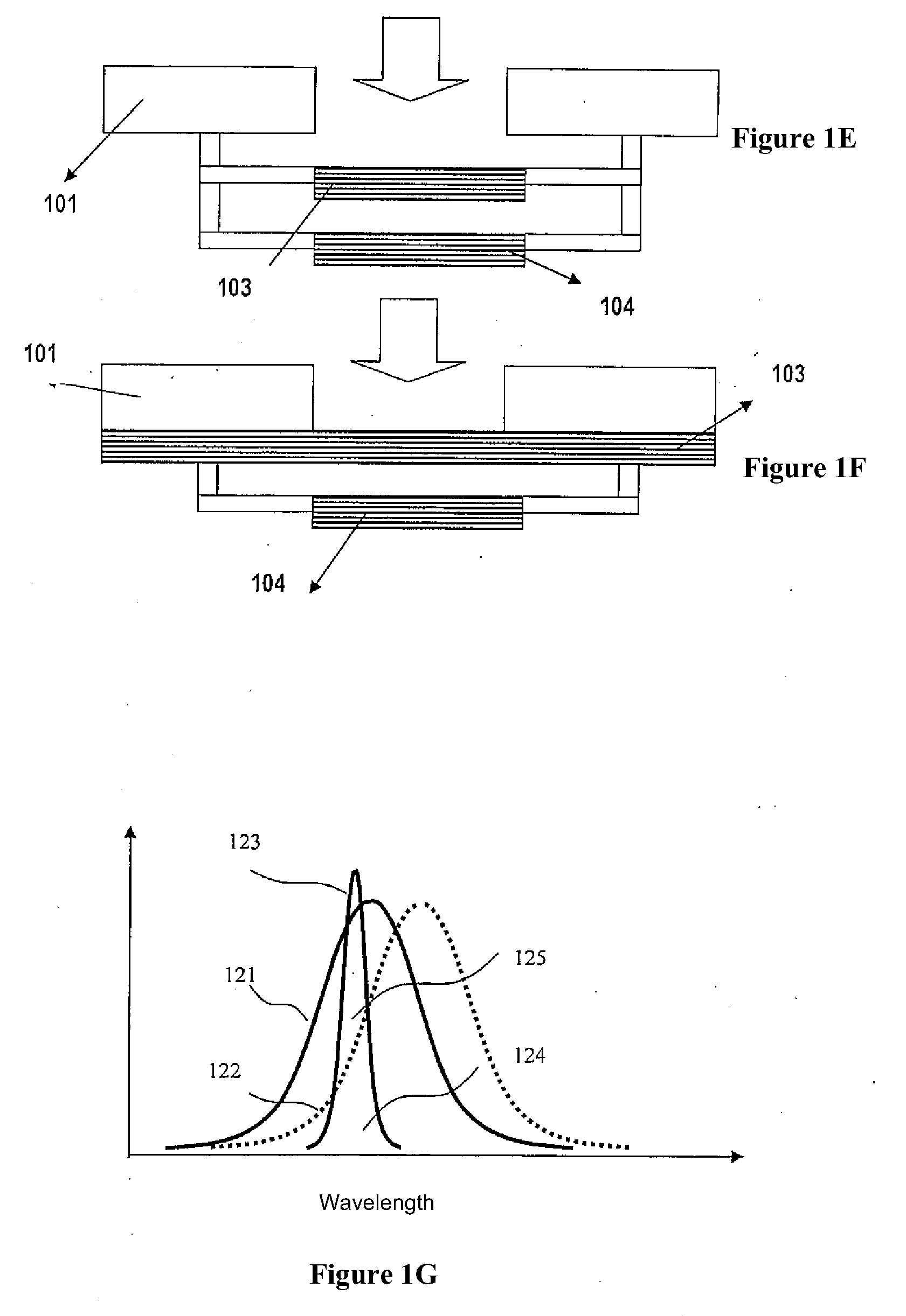
[0051]FIGS. 1A-C shows one embodiment of an infrared sensor described in this invention. As shown in FIGS. 1A-C, the infrared sensor comprises a substrate (101), a reflective layer (103) that is above the substrate or suspended above the substrate, a suspended reflective layer (104) that is above the reflective layer (103) and forms a gap between the suspending reflective layer (104) and the reflective layer (103), and a beam (106) which supports the reflective layer (104) over the substrate (101). Alternatively, beam (106) supports the reflective layer (104) over the reflective layer (103), as shown in FIG. 5B. In FIGS. 1A-C, the substrate (101) can be silicon or other semiconductor materials. If the infrared sensor operates at transmission mode, the substrate (101) needs to be transparent to the incident reference light (102). Preferably, substrate (101) can be glass, other trans...


PUM


Abstract

An infrared sensor and infrared imaging system, wherein said infrared sensor comprises: a first film structure, a second film structure, a gap between said first film structure and said second film structure. Reference light is incident from one of said first film structure and said second film structure. When said gap distance changes, the intensity of transmitted reference light changes, and the intensity of reflected reference light changes. When infrared light is incident, at least one of the said first and second film structures absorbs infrared light and the temperature changes, causing said gap distance to change. By detecting the intensity of said transmitted reference light or reflected reference light, the incident infrared light can be measured.

Description

TECHNICAL FIELDS[0001]This invention relates to infrared sensors, focal plane arrays and thermal imaging systems, especially infrared sensors, focal plane arrays and thermal imaging systems for detecting infrared lights emitted by objects.TECHNICAL BACKGROUND[0002]Infrared sensors detect infrared emission from objects at wavelength between about 8 μm to 14 μm that are not visible to human eyes, CCD or CMOS cameras. Traditional infrared sensors are fabricated using narrow band gap semiconductors or microbolometers, and they are difficult to make and expensive. Currently, there are some technologies that convert infrared signals into visible signals, and obtain the infrared image by calculating the infrared signal from the detected visible signals. One technology uses Micro-Electro-Mechanical Systems (MEMS) technology to manufacture infrared sensor array, i.e., focal plane array (FPA). In these structures, the supporting beams are made of different materials having different coefficie...

Claims


Application Information

Patent Timeline
Patent Type & Authority Applications(United States)
IPC IPC(8): G01J5/02
CPCG01J3/26G01J5/02G01J5/023G01J5/024G01J5/38G01J5/0853G01J5/0862G01J5/10G01J5/08G01J5/0802
Inventor SHEN, CHONGFEI
Owner SHANGHAI JUGE ELECTRONICS TECH
Why Eureka
Try Eureka