Method of Fabricating High Aspect Ratio Transducer Using Metal Compression Bonding

a transducer and metal compression technology, applied in the field of semiconductor devices, can solve the problems of difficult control of stress in the deposited layer, sensor sensitivity is limited, and the deposition-based fabrication technique is not well suited to forming high aspect ratio micro-electromechanical systems

Inactive Publication Date: 2010-08-05
FREESCALE SEMICON INC
View PDF19 Cites 259 Cited by
  • Summary
  • Abstract
  • Description
  • Claims
  • Application Information

AI Technical Summary

Problems solved by technology

While the deposition-based fabrication techniques have reduced the costs for making MEMS gyroscopes, there are difficulties associated with the various fabrication steps needed to build up the sensor component parts, including controlling the accuracy of the pattern and etch processes (e.g., in terms of the location, depth and width of etch openings) and the deposition processes (e.g., in terms of the location, thickness and width of defined features), as well as the structural integrity of the various sensor component parts.
The deposition-based fabrication techniques are also not well suited for forming high aspect ratio micro-electromechanical system (HARMEMS) devices which provide out-of-plane sensing and actuation performance.
And it is also difficult to control stress in the deposited layers.
However, these sensors have limited out-of-plane sensitivity due to limited electrode placement.

Method used


Image

  • Method of Fabricating High Aspect Ratio Transducer Using Metal Compression Bonding
  • Method of Fabricating High Aspect Ratio Transducer Using Metal Compression Bonding
  • Method of Fabricating High Aspect Ratio Transducer Using Metal Compression Bonding

Examples


Embodiment Construction

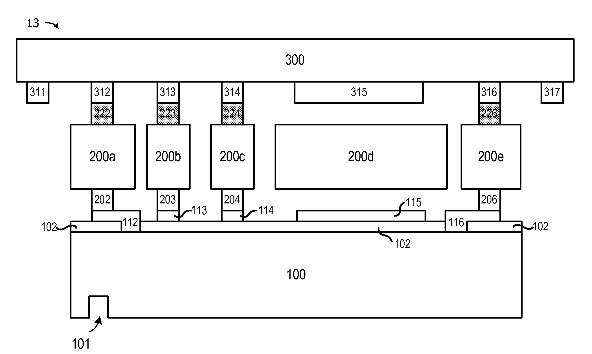
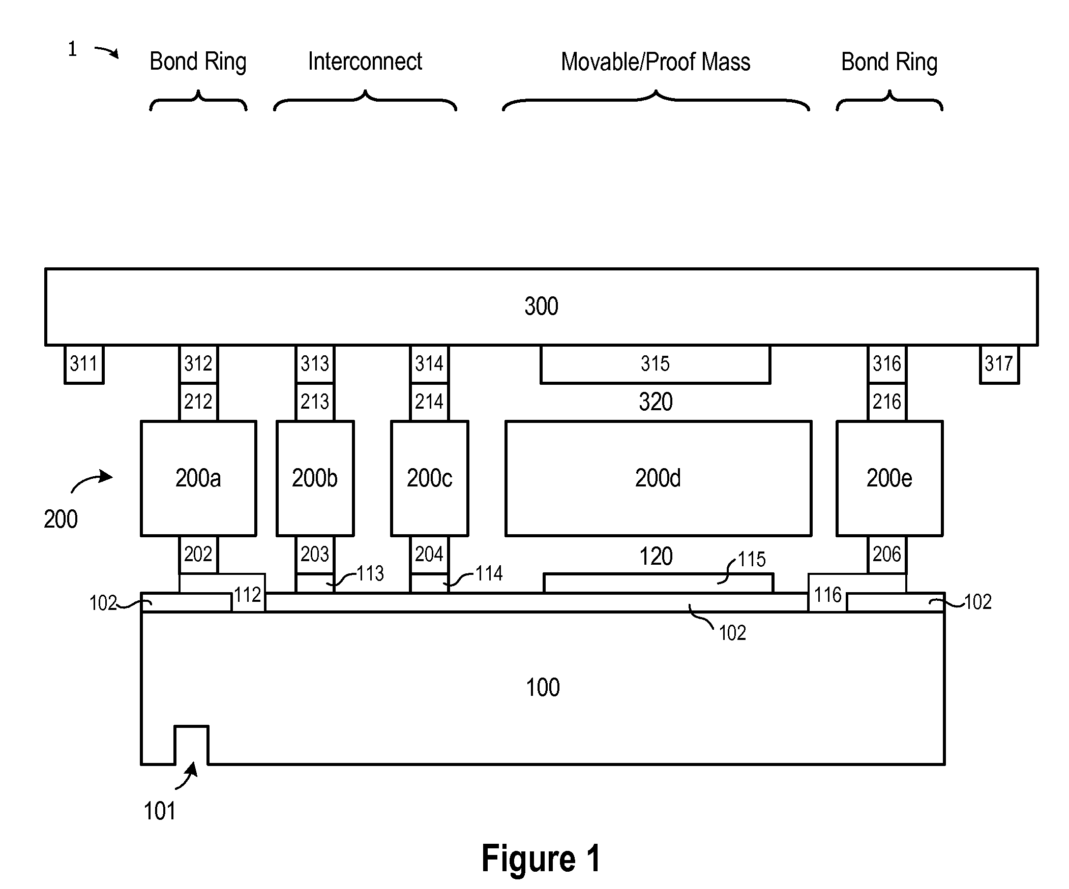
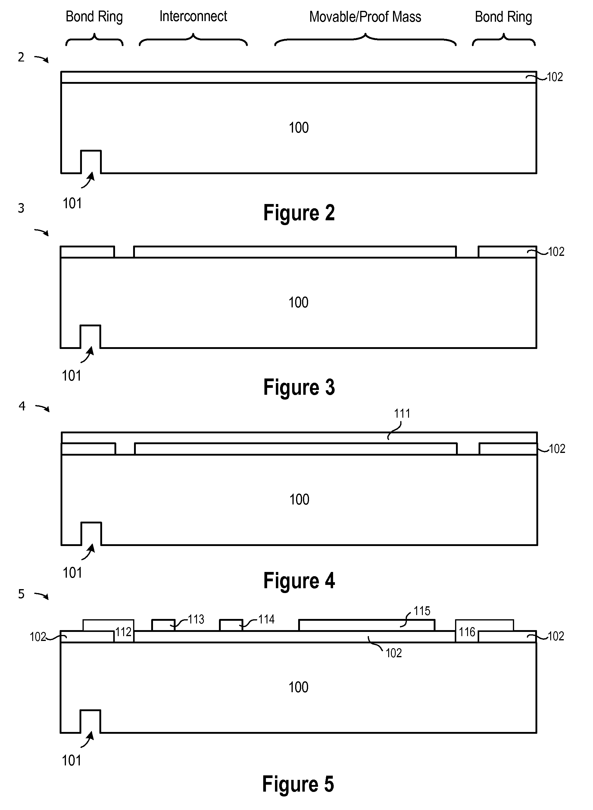
[0010]A method and apparatus are described for fabricating a high aspect ratio transducer using metal compression bonding to affix an active wafer to a reference wafer and a cap wafer. In selected embodiments, a first patterned layer of aluminum is formed on a monocrystalline silicon reference wafer to define electrode, interconnect, and bond ring structures. In addition, a second patterned layer of aluminum is formed on a first surface of a monocrystalline silicon active wafer to define aligned interconnect and bond ring structures so that the interconnect and bond ring structures on the active wafer and reference wafer can be aligned and bonded together using metal compression bonding techniques. After compression bonding the reference wafer to the active wafer, a third patterned layer of aluminum is formed on a second, opposite surface of the active wafer to define aligned interconnect and bond ring structures, or alternatively, a patterned layer of germanium is formed on the sec...


PUM


Abstract

A method and apparatus are described for fabricating a high aspect ratio MEMS device by using metal thermocompression bonding to assemble a reference wafer (100), a bulk MEMS active wafer (200), and a cap wafer (300) to provide a proof mass (200d) formed from the active wafer with bottom and top capacitive sensing electrodes (115, 315) which are hermetically sealed from the ambient environment by sealing ring structures (112 / 202 / 200a / 212 / 312 and 116 / 206 / 200e / 216 / 316).

Description

BACKGROUND OF THE INVENTION[0001]1. Field of the Invention[0002]The present invention is directed in general to the field of semiconductor devices. In one aspect, the present invention relates to MEMS devices and methods for fabricating MEMS devices.[0003]2. Description of the Related Art[0004]Micro-Electro-Mechanical Systems (MEMS) technology is increasingly used to integrate mechanical elements, sensors, actuators, and electronics on a common silicon substrate through microfabrication technology. For example, inertial sensors may be formed with MEMS devices on an integrated circuit wafer substrate to form various applications, such as a MEMS gyroscope that is used to measure an angular rate of an object. With conventional deposition-based fabrication techniques, a MEMS gyroscope is constructed from a silicon-on-insulator wafer that includes a substrate layer, a sacrificial layer overlying the substrate layer, and an active layer overlying the sacrificial layer, where trenches are ...

Claims


Application Information

Patent Timeline
Patent Type & Authority Applications(United States)
IPC IPC(8): B81B7/02H01L21/00H01L21/603H01L21/302H01L29/84G01P15/02
CPCB81B2201/025B81C1/00269G01P15/0802B81C2203/019B81C2203/0109
Inventor PARK, WOO TAELORECK, HEINZKARLIN, LISA
Owner FREESCALE SEMICON INC
Why Eureka
Try Eureka