Light/electric power converter and solid state imaging device

Inactive Publication Date: 2010-08-05
FUJIFILM CORP
View PDF13 Cites 6 Cited by
  • Summary
  • Abstract
  • Description
  • Claims
  • Application Information

AI Technical Summary

Benefits of technology

[0010]The other object of the present invention is to provide a light / electric power converter and a solid state imaging device that offer low cost.
[0018]According to the present invention, the structure is provided outside the active pixel area on the substrate. By planarizing the color filters to level with the structure, it is possible to precisely adjust the thickness of the color filter array. Additionally, the structure receives the heavy load of the planarizing steps, and prevents the intermediate layer of organic material from detaching. As a result, the production is improved, and the costs for the light / electric power converter and the solid state imaging device are reduced.

Problems solved by technology

The organic light / electric power converter, however, has a multilayer structure where the electrodes and the photoelectric conversion layer are stacked on the semiconductor substrate, creating an uneven surface between the semiconductor substrate and the color filters.
However, this time control method does not guarantee a uniform layer thickness of the light / electric power converters, particularly when the speed of the polishing or etching operation fluctuates.

Method used


Image

  • Light/electric power converter and solid state imaging device
  • Light/electric power converter and solid state imaging device
  • Light/electric power converter and solid state imaging device

Examples


Embodiment Construction

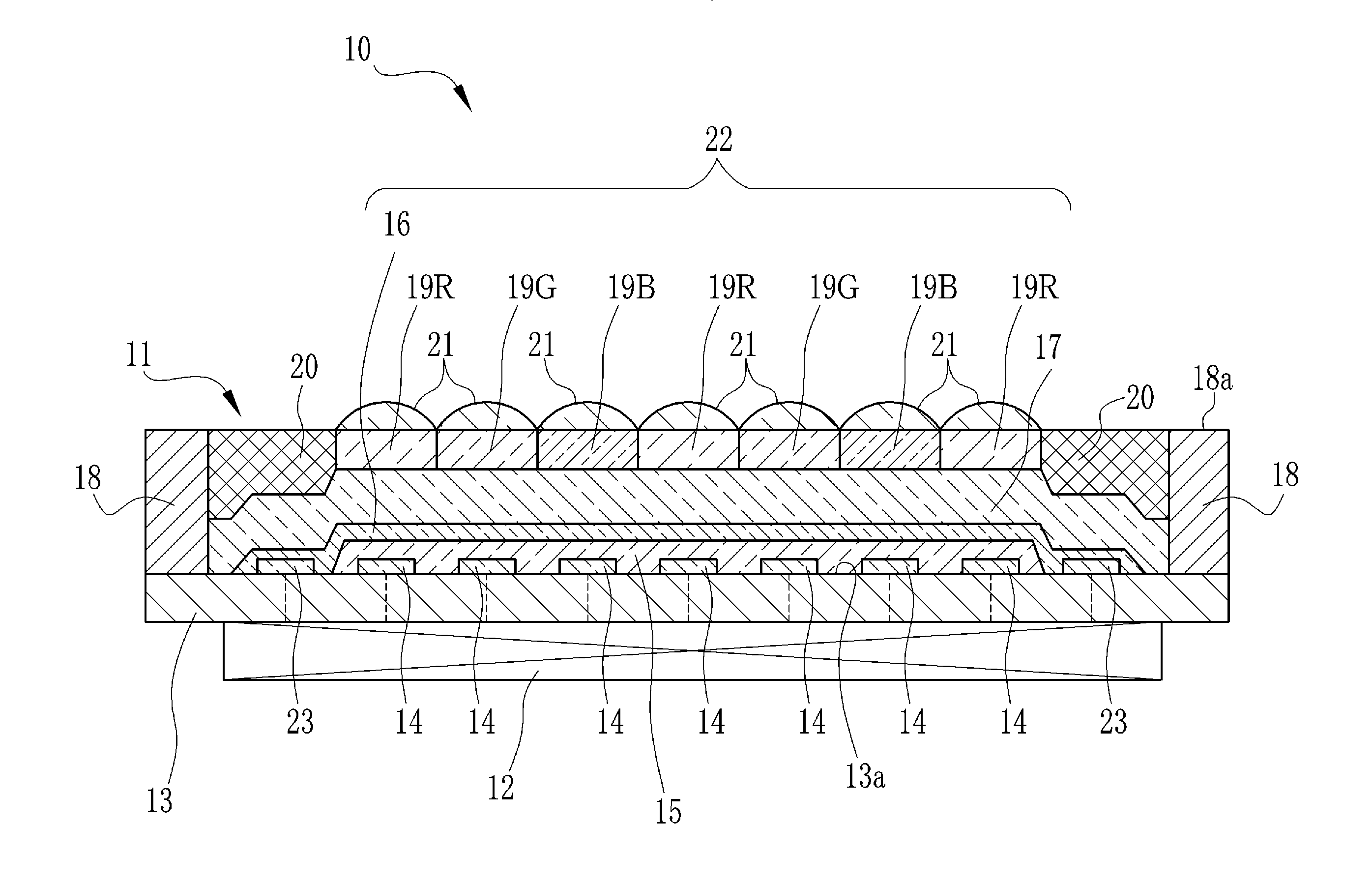
[0052]Referring to FIG. 1, a solid state imaging device 10 has a light / electric power converter 11 and a drive circuit 12. The light / electric power converter 11 includes a semiconductor substrate 13 having a top surface 13a as a reference plane, a plurality of lower electrodes 14 on the top surface 13a, an intermediate layer 15 covering the lower electrodes 14, an upper electrode 16 on the intermediate layer 15, a transparent insulating layer 17 covering the upper electrode 16, a polish stop layer (structure) 18 on the top surface 13a, an array of color filters 19R, 19G and 19B, a light shield layer 20 surrounding the color filter array, and an array of micro-lenses 21 on the color filters 19R, 19G and 19B. The overlap of the lower electrode 14, the intermediate layer 15, the upper electrode 16, one of the color filters 19R, 19G and 19B and one of the micro-lenses 21 constitutes a single pixel. These pixels are arranged in a mosaic pattern to form an active pixel area 22.

[0053]The c...


PUM


Abstract

A semiconductor substrate has an active pixel area comprising a stack of lower electrodes, an intermediate layer of an organic photoelectric conversion material, an upper electrode, a transparent insulating layer and first to third color layers. Disposed outside the active pixel area is a polish stop layer having a high resistance to polishing. In planarizing the first to third color layers, the polishing operation is ended upon reaching the polish stop layer.

Description

FIELD OF THE INVENTION[0001]The present invention relates to a light / electric power converter having a polish stop layer outside an active pixel area, and a solid state imaging device equipped with this light / electric power converter.BACKGROUND OF THE INVENTION[0002]Current solid state imaging devices become to have an ever-smaller light receiving area per one pixel so as to increase the number of pixels. Such downsizing of the light receiving area causes color mixture between adjacent pixels, and the solid state imaging devices need to have a color filter with excellent color separation capability to suppress the color mixture. The color filter is generally formed by a photolithography method or a dry etching method.[0003]The photolithography method, which is compatible with a photolithography process in the semiconductor manufacture, allows for reducing initial investment, and is therefore widely used for forming the color filter. The color filter formation using the photolithogra...

Claims


Application Information

Patent Timeline
IPC IPC(8): H04N5/335H01L27/14H01L27/146H01L31/0232
CPCH01L27/14618H01L27/14621H04N9/045H01L27/14683H01L27/14627H01L2924/0002H01L27/14623H04N25/11H01L2924/00
Inventor MAEHARA, YOSHIKIYOSHIBAYASHI, MITSUJI
Owner FUJIFILM CORP
Why Eureka
Try Eureka