Magnetoresistive element and method of manufacturing the same

a technology of magnetoresistive elements and magnetoresistive elements, which is applied in the manufacture of inductance/transformer/magnets, magnetic bodies, solid-state devices, etc., can solve the problems of failure of the magnetoresistive element and the mram, the failure of the magnetoresistive element and the use of the mram, and the difficulty of both achieving the miniaturization of the memory cell toward an increase in capacity

Active Publication Date: 2010-08-12
KIOXIA CORP
View PDF14 Cites 68 Cited by
  • Summary
  • Abstract
  • Description
  • Claims
  • Application Information

AI Technical Summary

Benefits of technology

[0026]FIG. 12 is an explanatory diagram of en effect of the magnetoresistive element according to the first embodiment;

Problems solved by technology

With the magnetic field write type MRAM, it is difficult both to achieve miniaturization of a memory cell toward an increase in capacity and to reduce power consumption of the memory cell.
This is a cause of failure of the magnetoresistive element and an MRAM using it.
In Jpn. Pat. Appln. KOKAI Publication No. 2005-44848, however, an effect of removing the residue f

Method used


Image

  • Magnetoresistive element and method of manufacturing the same
  • Magnetoresistive element and method of manufacturing the same
  • Magnetoresistive element and method of manufacturing the same

Examples


first embodiment

1. First Embodiment

[0036]Referring to FIGS. 1 to 13, a first embodiment of the invention is described below.

[0037](1) Structure

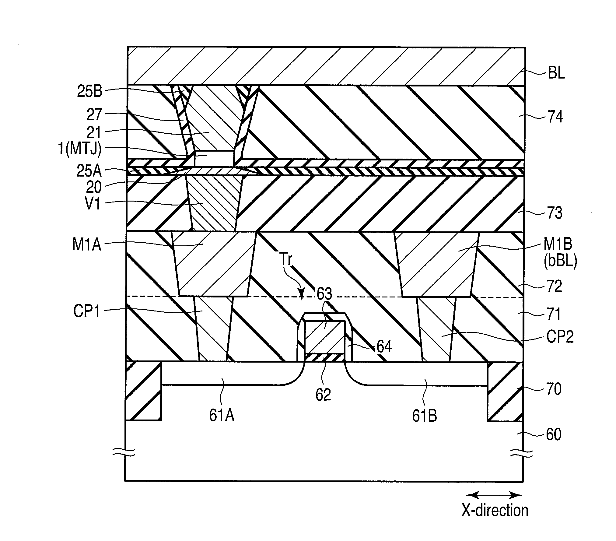
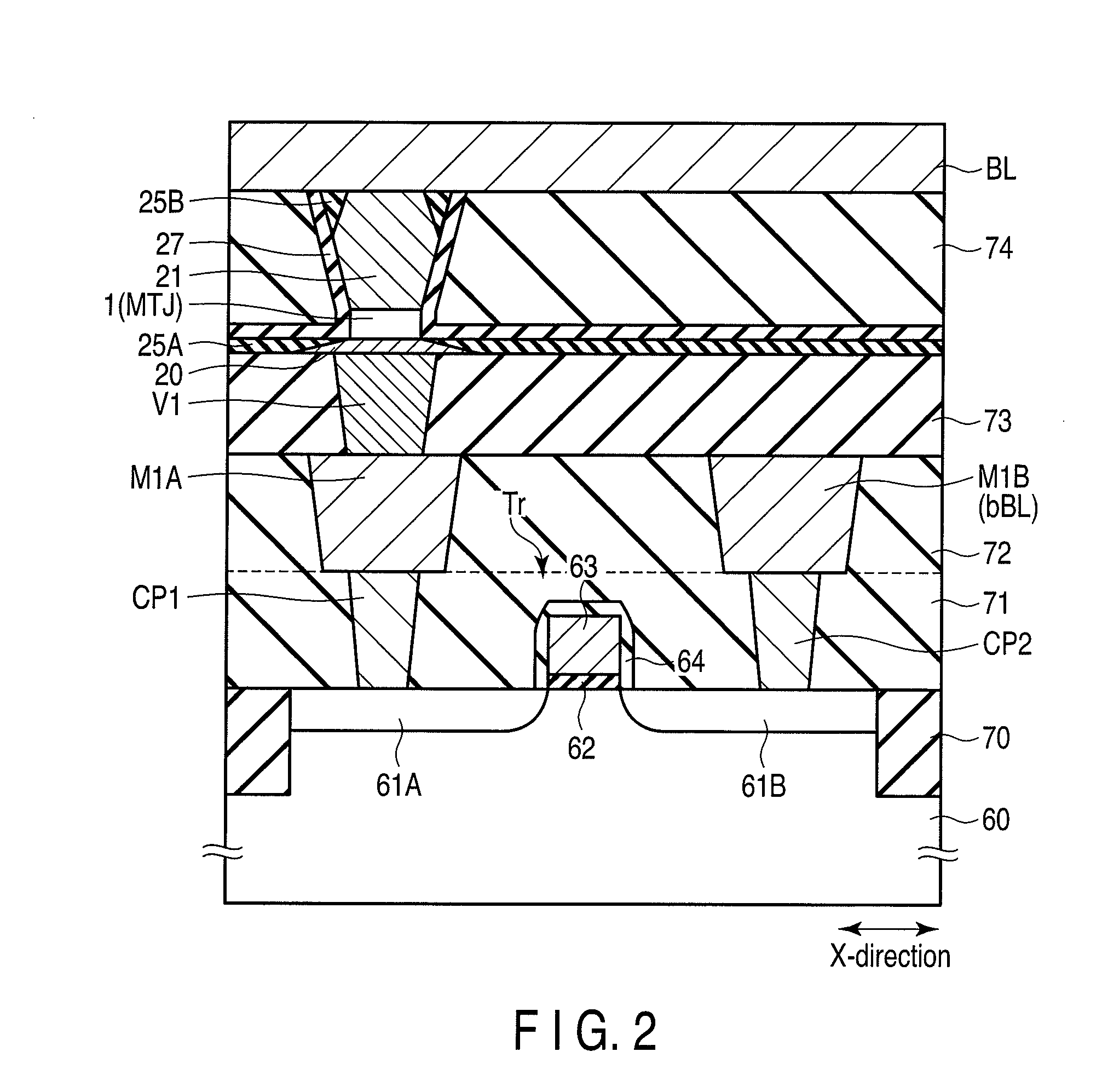
[0038]Referring to FIGS. 1 to 4, a structure of a magnetoresistive element according to the first embodiment of the invention is described.

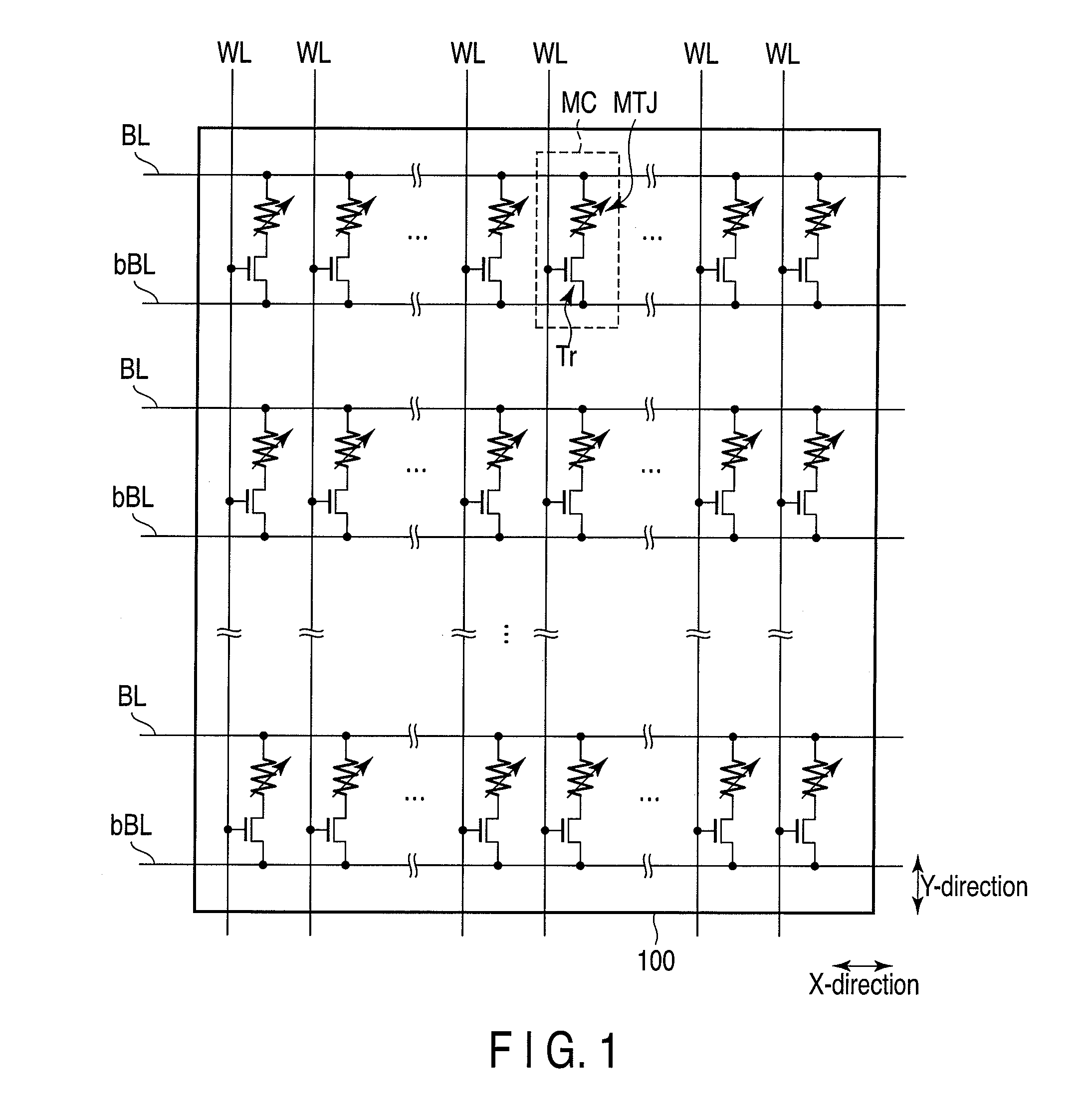
[0039]FIG. 1 shows an equivalent circuit of a memory cell array of a magnetic random access memory (MRAM).

[0040]In a memory cell array 100, a plurality of bit lines BL and bBL extending in the X-direction and a plurality of word lines WL extending in the Y line are provided. Connected to one memory cell MC are one word line WL and two bit lines BL and bBL. The two bit lines BL and bBL form a pair of bit lines.

[0041]In the memory cell array 100, a plurality of memory cells MC are arranged in an array configuration. The plurality of memory cells MC arranged along the X-direction are commonly connected to a pair of bit lines BL and bBL. The plurality of memory cells MC arranged along the Y-direction are commonly connected to...

second embodiment

2. Second Embodiment

[0144]Referring to FIGS. 14 to 19, a second embodiment of the invention is described below. Note that, in the second embodiment, components identical or equivalent to those described in the first embodiment are indicated by the same reference characters, and their detailed descriptions are given as necessary.

[0145](1) Structure

[0146]Referring to FIG. 14, a structure of a magnetoresistive element according to the second embodiment of the invention is described.

[0147]FIG. 14 shows a structure of a magnetoresistive element according to this embodiment. Configurations of a memory cell and a memory cell array in which the magnetoresistive element is used are the same as those shown in FIGS. 1 and 2, and therefore their descriptions are omitted here.

[0148]As shown in FIG. 14, in the magnetoresistive element 1 of this embodiment, the structure of the upper electrode 21Y differs from that of a magnetoresistive element of the first embodiment.

[0149]In this embodiment, the...

third embodiment

3. Third Embodiment

[0169]Referring to FIG. 20, a structure of a magnetoresistive element according to a third embodiment of the invention is described. Note that, in the third embodiment, components identical or equivalent to those described in the first embodiment are indicated by the same reference characters, and their detailed descriptions are given as necessary.

[0170]In the first and second embodiments, the structure of the magnetoresistive element 1 is a three-layer structure in which three films are laminated. However, the structure of the magnetoresistive element is not limited to the three-layer structure and may be a laminated structure including four or more layers.

[0171]As shown in FIG. 20, a magnetoresistive element 10 may have a double-junction structure. The magnetoresistive element 10 of the double-junction structure comprises a ferromagnetic layer of a first magnetic pinned layer 11X, a first tunnel barrier layer 12X, a ferromagnetic layer of the magnetic free layer...


PUM


Abstract

A magnetoresistive element of an aspect of the present invention including a lower electrode provided on an insulating layer on a semiconductor substrate, a first ferromagnetic layer provided on the lower electrode, a first tunnel barrier layer provided on the first ferromagnetic layer, a second ferromagnetic layer provided on the first tunnel barrier layer, and an upper electrode provided on the second ferromagnetic layer, wherein the upper electrode has a hexagonal cross-sectional shape, and a maximum size of the upper electrode in a first direction is larger than a size of the first tunnel barrier layer in the first direction, the first direction being horizontal relative to a surface of the semiconductor substrate.

Description

CROSS-REFERENCE TO RELATED APPLICATIONS[0001]This application is based upon and claims the benefit of priority from prior Japanese Patent Application No. 2009-030105, filed Feb. 12, 2009, the entire contents of which are incorporated herein by reference.BACKGROUND OF THE INVENTION[0002]1. Field of the Invention[0003]The present invention relates to a magnetoresistive element and a method of manufacturing the magnetoresistive element.[0004]2. Description of the Related Art[0005]A magnetoresistive random access memory (MRAM) is a nonvolatile semiconductor memory which stores data using a variation in resistance of a magnetoresistive element due to a change in relative relationship between directions of magnetization of two ferromagnetic layers included in the magnetoresistive element.[0006]A memory cell of an MRAM includes a magnetoresistive element in which a plurality of ferromagnetic layers and a barrier layer are laminated. The magnetoresistive element comprises a ferromagnetic la...

Claims


Application Information

Patent Timeline
IPC IPC(8): H01L29/82H01L21/8246
CPCB82Y25/00B82Y40/00H01F10/3254H01L43/12H01F41/308H01L27/228H01L43/08H01F41/307H10B61/22H10N50/10H10N50/01
Inventor IWAYAMA, MASAYOSHI
Owner KIOXIA CORP
Why Eureka
Try Eureka