Display device

a technology of a display device and a display screen, which is applied in the field of display devices, can solve the problems of poor crack prevention effect insufficient adhesion between the respective layers, and insufficient satisfaction of the structure illustrated in fig. 12 or fig. 13 of the barrier layer, and achieve the enhancement of the barrier property and the reduction of the light reflectance of the barrier layer

Inactive Publication Date: 2010-08-12
PANASONIC LIQUID CRYSTAL DISPLAY CO LTD +1
View PDF4 Cites 12 Cited by
  • Summary
  • Abstract
  • Description
  • Claims
  • Application Information

AI Technical Summary

Benefits of technology

[0025]The display device having the structures as described above, which includes the barrier layer having the laminate structure formed of the plurality of material layers, is capable of reducing the light reflectance of the barrier layer and also achieving the crack prevention, the adhesion between the respective layers, and the enhancement in barrier property.

Problems solved by technology

However, for the purpose of reducing the light reflectance, when the structure illustrated in FIG. 14 is adopted without any modification, excellent effects may not be obtained in terms of the crack prevention of the barrier layer, the adhesion between the respective layers, and the barrier property.
This is because, in the case where the refractive indexes of the respective layers are changed in a stepwise manner, densities and stresses of the respective layers generally become higher along with the increase in refractive indexes thereof, with the result that the structure illustrated in FIG. 12 or FIG. 13 may not be satisfied.

Method used


Image

  • Display device
  • Display device
  • Display device

Examples


first embodiment

Schematic Structure of Display Device

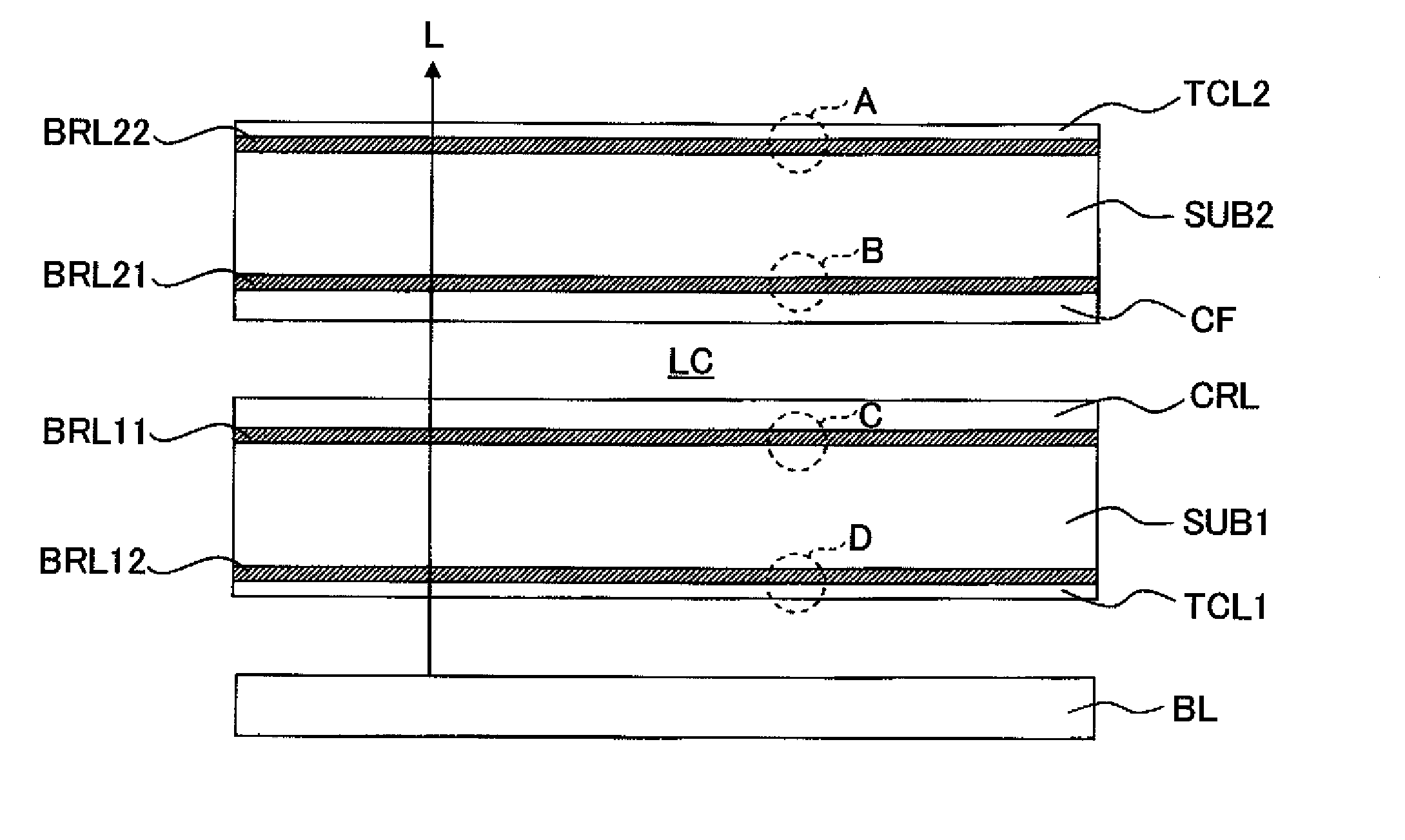
[0043]FIG. 2 is a cross-sectional view schematically illustrating a display device according to the present invention by taking a liquid crystal display device (panel) as an example.

[0044]In FIG. 2, a substrate SUB1 and a substrate SUB2 are disposed so as to be opposed to each other with liquid crystal LC being sandwiched therebetween. The substrate SUB1 and the substrate SUB2 are both formed of a plastic substrate made of a flexible resin material.

[0045]A barrier layer BRL11 is formed on a liquid-crystal-side surface of the substrate SUB1. The barrier layer BRL11 prevents moisture from permeating the substrate SUB1. A circuit structure layer CRL including a thin film transistor (not shown) is formed on an upper surface of the barrier layer BRL11. The circuit structure layer CRL includes, in each of pixel regions arranged in matrix, a pair of electrodes (pixel electrode and counter electrode) for generating an electric field in the liquid crystal...

second embodiment

[0067]The first embodiment describes the case that the present invention is applied to a liquid crystal display device. However, the present invention is not limited thereto, and may be applied to other display device such as an organic electroluminescence (EL) display device.

[0068]FIG. 6 is a cross-sectional view schematically illustrating an organic EL display device. FIG. 6 illustrates a substrate SUB, which is made of a flexible resin material. A barrier layer BRL1 is formed on one surface (main surface) of the substrate SUB, and a barrier layer BRL2 is formed on another surface thereof. The barrier layer BRL1 and the barrier layer BRL2 prevent moisture from permeating the substrate SUB. A circuit structure layer CRL including a thin film transistor (not shown) is formed on an upper surface of the barrier layer BRL1. A cathode electrode KT is formed in each of pixel regions arranged in matrix on an upper surface of the circuit structure layer CRL. A light emitting layer EL is fo...

third embodiment

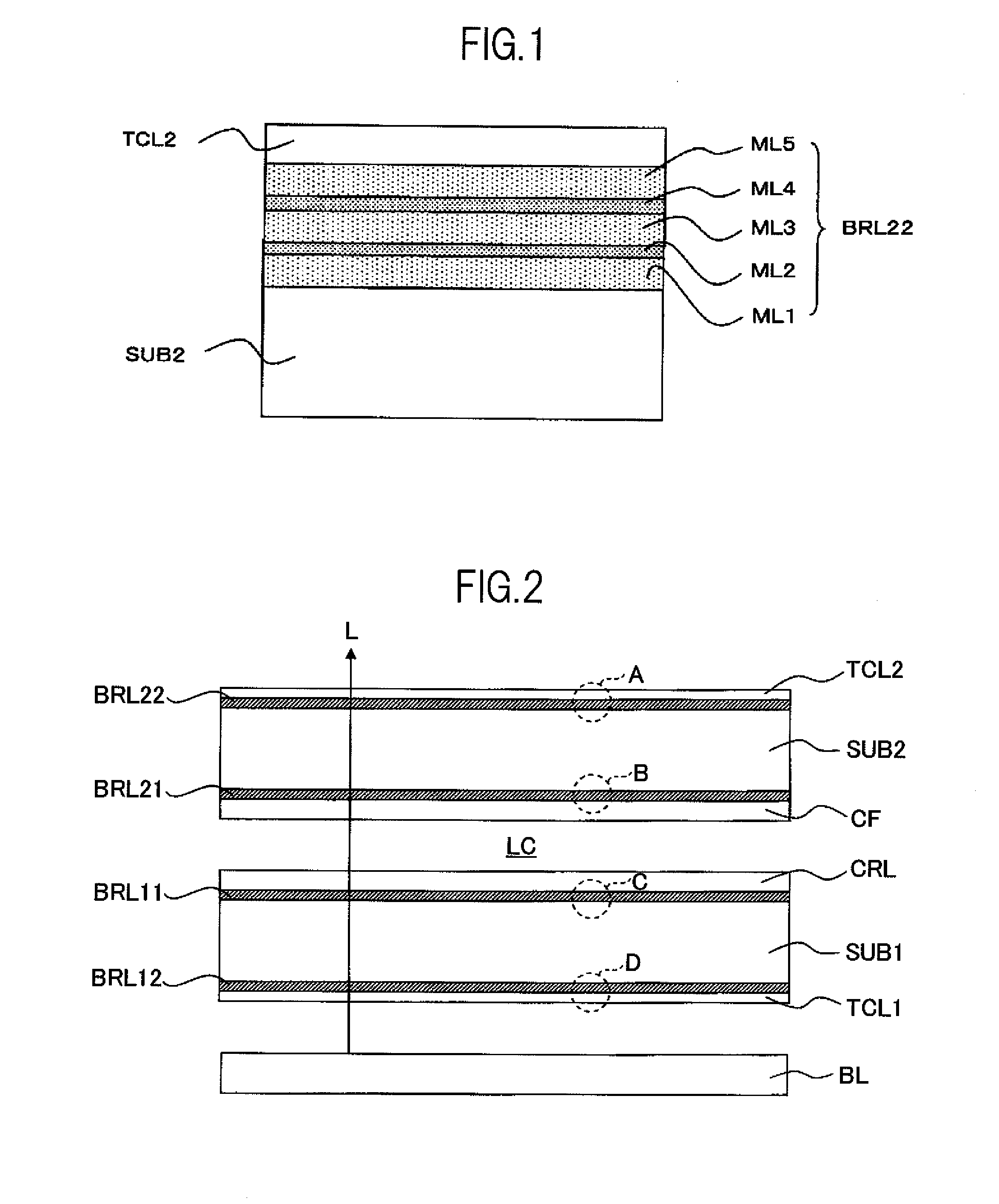
[0071]In the barrier layer BRL of the above-mentioned embodiments, the respective material layers ML which are laminated on each other are made of an insulating material such as SiON. Alternatively, at least one of the material layers ML may be formed of a conductive layer. The conductive layer may be made of, for example, a conductive polymer.

[0072]The reason for this is as follows. For example, when the above-mentioned structure is applied to the barrier layer BRL11 formed below the circuit structure layer CRL of FIG. 2 or the barrier layer BRL1 formed below the circuit structure layer CRL of FIG. 6 or 7, an effect of reducing a threshold voltage shift (ΔVth) of the thin film transistor included in the circuit structure layer CRL may be achieved. In this case, the conductive layer may be grounded or may not be grounded. This is because, in both of the cases, the threshold voltage shift (ΔVth) of the thin film transistor may be reduced.


PUM

PropertyMeasurementUnit
light refractive indexaaaaaaaaaa
pressureaaaaaaaaaa

Abstract

Provided is a display device, including: a barrier layer formed of a plurality of material layers being laminated; and a first material layer and a second material layer that sandwich the barrier layer, in which: the first material layer, the plurality of material layers forming the barrier layer, and the second material layer have light refractive indexes that are set so as to sequentially change from the first material layer to the second material layer in one of decreasing order and increasing order; and the plurality of material layers forming the barrier layer include a high stress film and a low stress film which are alternately laminated on each other. Therefore, the display device of the present invention can achieve crack prevention, enhancement in adhesion between the respective layers and enhancement in barrier property, together with reducing a light reflectance of the barrier layer.

Description

CROSS-REFERENCE TO RELATED APPLICATION[0001]The present application claims priority from Japanese application JP2009-027191 filed on Feb. 9, 2009, the content of which is hereby incorporated by reference into this application.BACKGROUND OF THE INVENTION[0002]1. Field of the Invention[0003]The present invention relates to a display device, and more particularly, to a display device including a substrate formed of a flexible plastic substrate.[0004]2. Description of the Related Art[0005]In a display device including a substrate formed of a flexible plastic substrate, the substrate is more light in weight and has higher impact resistance and flexibly compared with a substrate made of, for example, glass.[0006]However, the plastic substrate has higher hygroscopicity and a property of expanding upon absorbing moisture compared with the glass substrate, and hence it is required to form a barrier film for preventing moisture from permeating the plastic substrate, on a surface of the plasti...

Claims


Application Information

Patent Timeline
Patent Type & Authority Applications(United States)
IPC IPC(8): G02F1/1333G02B27/00
CPCG02B1/105G02F1/133305G02F2201/503G02F2201/50G02F2201/38G02B1/16G02B1/14
Inventor OKADA, NAOYAHATANO, MUTSUKOYAMAGUCHI, SHINYAHATTORI, TAKASHI
Owner PANASONIC LIQUID CRYSTAL DISPLAY CO LTD
Why Eureka
Try Eureka