
Light emitting and lasing semiconductor devices and methods

a technology of semiconductor devices and semiconductor components, applied in semiconductor devices, semiconductor lasers, lasers, etc., can solve the problems of reducing the quantum efficiency of the described devices and saturating behavior, and achieve the effect of reducing quantum efficiency and minimizing the non-radiative recombination componen

Active Publication Date: 2010-08-12
THE BOARD OF TRUSTEES OF THE UNIV OF ILLINOIS +1
View PDF16 Cites 34 Cited by
  • Summary
  • Abstract
  • Description
  • Claims
  • Application Information

AI Technical Summary

Benefits of technology

[0011]Applicant believes that one of the main factors leading to the saturation behavior and reduced quantum efficiency in the described devices is the rethermalization of carriers back towards the emitter side (back diffusion). Therefore, in accordance with a feature hereof, an asymmetric base design is employed to minimize the non-radiative recombination component due to the back diffusion of carriers.
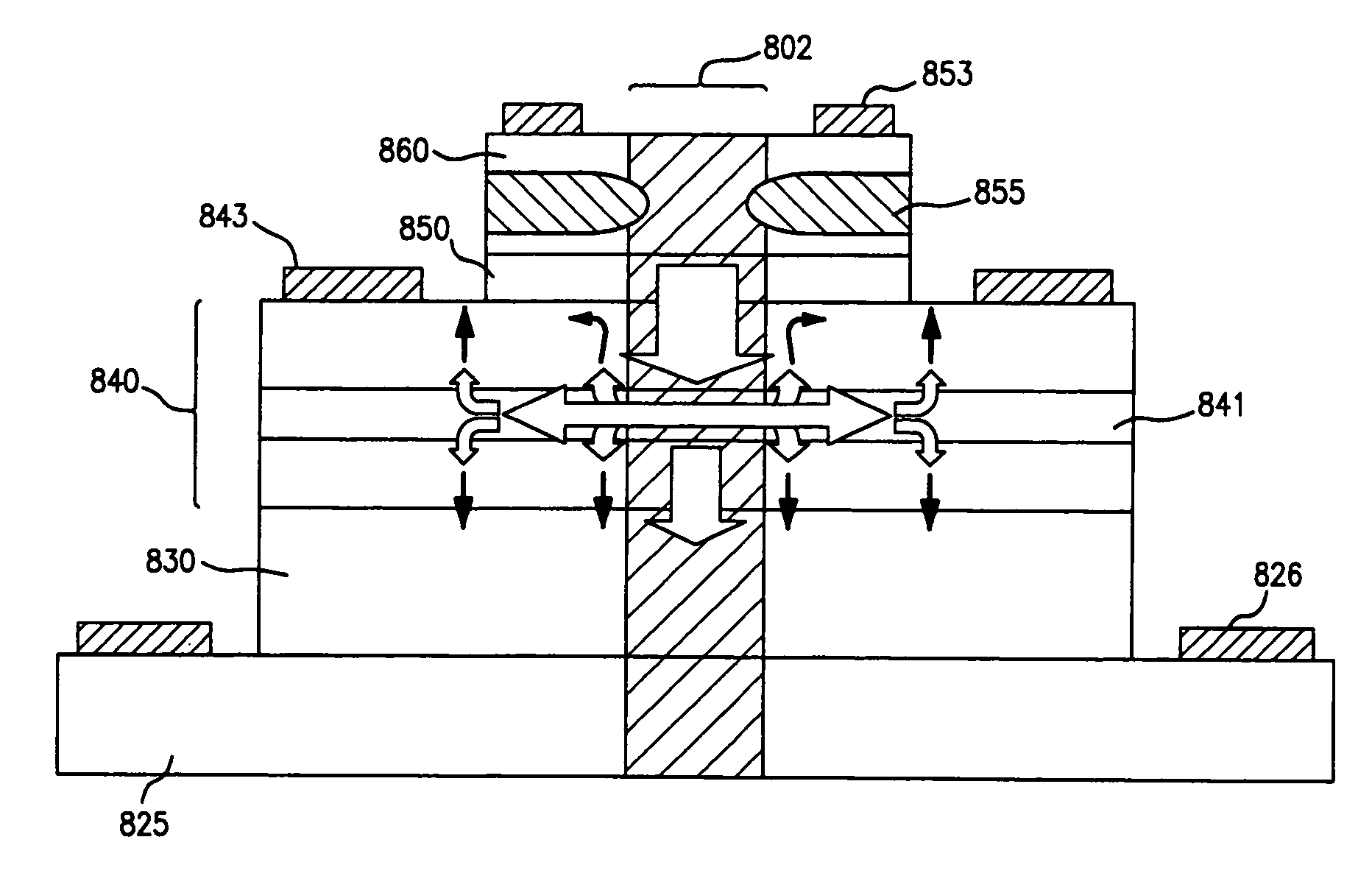
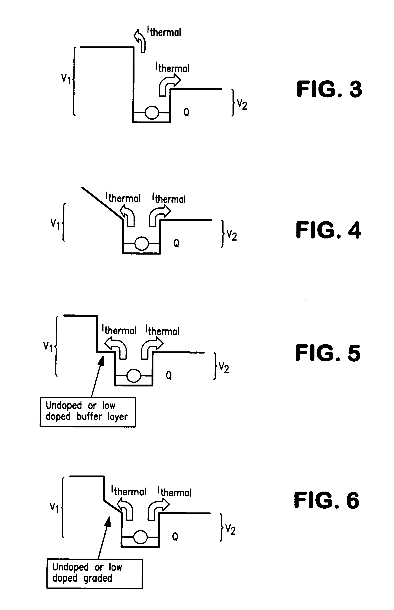
[0012]In accordance with a form of the invention, a method is set forth for improving operation of a light emitting transistor, including the following steps: providing a light emitting transistor that includes emitter, base, and collector semiconductor regions, and a quantum size region within the base region, the base region comprising a first base sub-region on the emitter side of said quantum size region, and a second base sub-region on the collector side of said quantum size region; and providing said first and second base sub-regions with asymmetrical band structures. In an embodiment of this form of the invention, the step of providing the first and second base sub-regions with asymmetrical band structures comprises providing the first base sub-region with a higher bandgap semiconductor material than the semiconductor material of the second base sub-region. In one version of this embodiment, the step of providing the first base sub-region with a higher bandgap semiconductor material than the semiconductor material of the second base sub-region includes providing the first base sub-region with a graded bandgap semiconductor material. The graded bandgap semiconductor material is graded to have a gradually increasing bandgap in the direction of said emitter. In another version of this embodiment, the step of providing the first base sub-region with a higher bandgap semiconductor material than the semiconductor material of the second base sub-region includes providing the first base sub-region with a stepped bandgap semiconductor material. In a further version of this embodiment, the step of providing the first base sub-region with a higher bandgap semiconductor material than the semiconductor material of the second base sub-region includes providing the first base sub-region with a graded and stepped bandgap semiconductor material.

Problems solved by technology

Applicant believes that one of the main factors leading to the saturation behavior and reduced quantum efficiency in the described devices is the rethermalization of carriers back towards the emitter side (back diffusion).

Method used


Image

  • Light emitting and lasing semiconductor devices and methods
  • Light emitting and lasing semiconductor devices and methods
  • Light emitting and lasing semiconductor devices and methods

Examples


Embodiment Construction

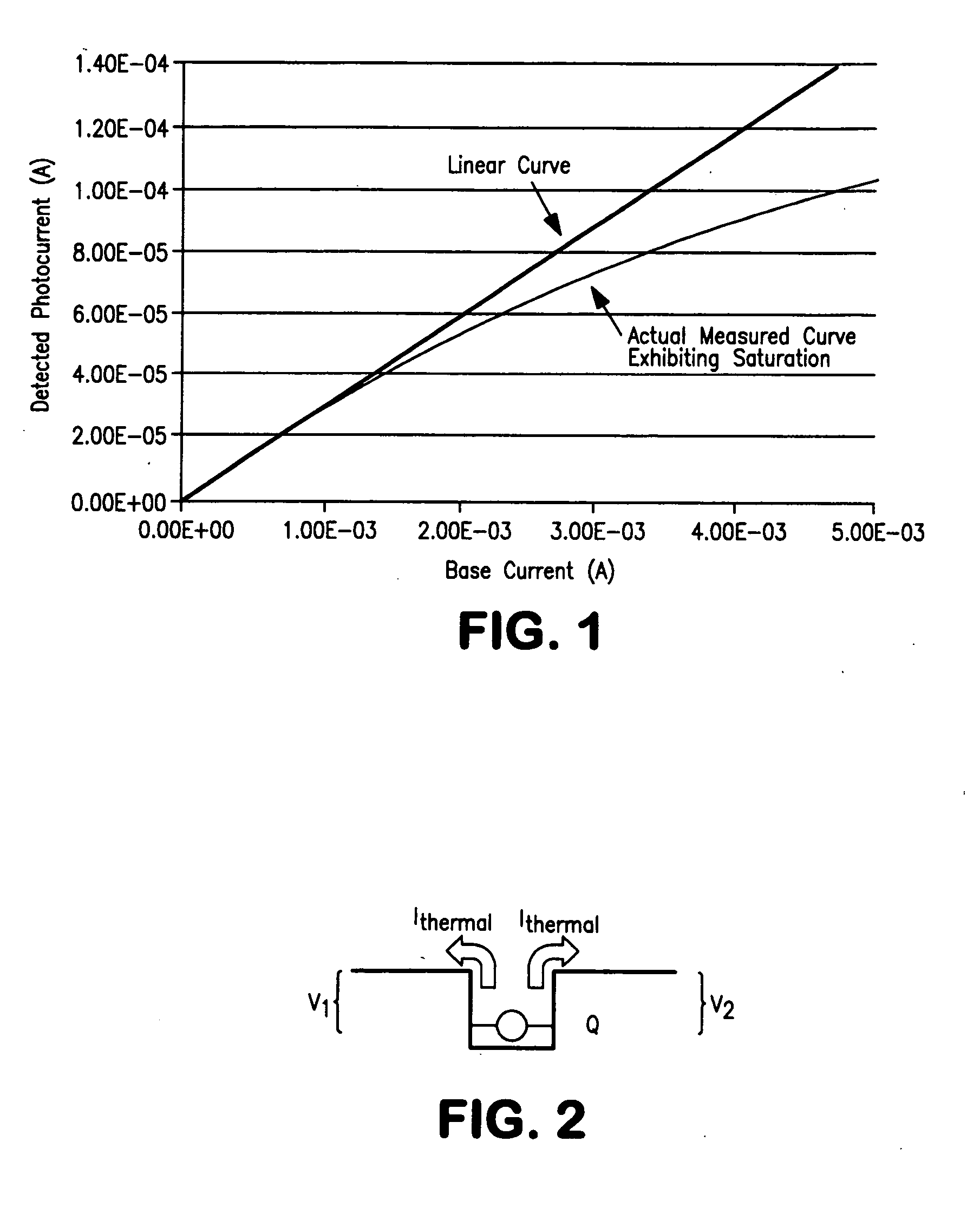
[0031]Applicant has observed that the radiative recombination component does not increase linearly with base current. FIG. 1 shows measured photon output from a QW-HBLET exhibiting saturation behavior (departure from linear curve) at higher base current indicating an increase in non-radiative recombination component. In addition, Applicant has also observed that the radiative recombination component is also a strong function of temperature. These observations further suggest that non-radiative recombination activity, and therefore bulk base recombination, also increases as a function of both current density and temperature.

[0032]Referring to FIG. 2, which shows an energy band diagram for a typical quantum well in a base region, the thermalization current (Ithermal) depends mainly on two variables, phonon energy (proportionate to temperature, T) and the barrier height (V) in which the carriers are confined, as seen from the following relationships:

Ithermal1∝-qV1kTIthermal2∝-qV2kTIthe...


PUM


Abstract

A semiconductor light emitting device, including: a heterojunction bipolar light-emitting transistor having a base region between emitter and collector regions; emitter, base, and collector electrodes for coupling electrical signals with the emitter, base, and collector regions, respectively; and a quantum size region in the base region; the base region including a first base sub-region on the emitter side of the quantum size region, and a second base sub-region on the collector side of the quantum size region; and the first and second base sub-regions having asymmetrical band structures.

Description

PRIORITY CLAIMS[0001]Priority is claimed from U.S. Provisional Patent Application Ser. No. 61 / 204,560, filed Jan. 8, 2009, and from U.S. Provisional Patent Application Ser. No. 61 / 204,602, filed Jan. 8, 2009, and from U.S. Provisional Patent Application Ser. No. 61 / 208,422, filed Feb. 24, 2009, and all of said U.S. Provisional Patent Applications are incorporated herein by reference.RELATED APPLICATION[0002]The subject matter of this application relates to subject matter disclosed in copending U.S. patent application Ser. No. ______, filed of even date herewith and assigned to the same assignees as the present application.FIELD OF THE INVENTION[0003]This invention relates to methods and devices for producing light emission and laser emission in response to electrical signals. The invention also relates to methods for producing light emission and laser emission from semiconductor transistor devices with improved efficiency.BACKGROUND OF THE INVENTION[0004]A part of the background her...

Claims


Application Information

Patent Timeline
IPC IPC(8): H01S5/34H01L33/04
CPCB82Y20/00H01S5/06203H01S5/34313H01S5/3412H01S5/18311
Inventor HOLONYAK, JR., NICKFENG, MILTONWALTER, GABRIEL
Owner THE BOARD OF TRUSTEES OF THE UNIV OF ILLINOIS
Learn More