Output buffer circuit

a buffer circuit and output technology, applied in the field can solve the problems of low response speed of output buffer circuits, and achieve the effect of reducing output noise and less influence on output nois

Inactive Publication Date: 2010-08-19
SEIKO INSTR INC
View PDF0 Cites 5 Cited by
  • Summary
  • Abstract
  • Description
  • Claims
  • Application Information

AI Technical Summary

Benefits of technology

[0017]The present invention has been made in view of the above-mentioned problem, and an object of the present invention is to provide an output buffer circuit capable of reducing output noise and suppressing a delay of a response speed.
[0023]According to the present invention, in a range including a voltage ½ times a power supply voltage that is likely to generate output noise (in a range out of a predetermined range), the logic circuit having a predetermined driving ability or less is used, and the first transistors or the second transistors in a number smaller than a predetermined number are turned on. Therefore, the slew rate of an output voltage becomes gentle, to thereby reduce output noise.
[0024]On the other hand, in a predetermined range excluding a voltage ½ times a power supply voltage having less influence on output noise, even if the logic circuit having a predetermined driving ability or less is used, the first transistors or the second transistors in a predetermined number (at least two) are turned on. This prevents the slew rate of an output voltage from becoming steep to delay the response speed of the output buffer circuit.

Problems solved by technology

Therefore, a response speed of the output buffer circuit becomes low.

Method used


Image

  • Output buffer circuit
  • Output buffer circuit
  • Output buffer circuit

Examples


embodiment

(1) Outline of Embodiment

[0036]In an output buffer circuit of this embodiment, in the same way as in the conventional art, the driving ability of a logic circuit that drives a transistor in an output stage is designed to be smaller than that of an ordinary logic circuit, to thereby decrease the driving current from the logic circuit to a gate of the transistor in the output stage, and reduce a change amount of a gate voltage of the transistor in the output stage. Thus, a change amount of an output current of the transistor in the output stage is small, and the slew rate of the output voltage of the transistor in the output stage becomes gentle, and hence, output noise is reduced.

[0037]On the other hand, when the slew rate of the output voltage of the transistor in the output stage is rendered gentle with respect to the entire range in which the output voltage changes, there arises a problem of a delay of a response speed of the output buffer circuit.

[0038]In this embodiment, the fac...

first embodiment

[0040]First, a configuration of an output buffer circuit is described.

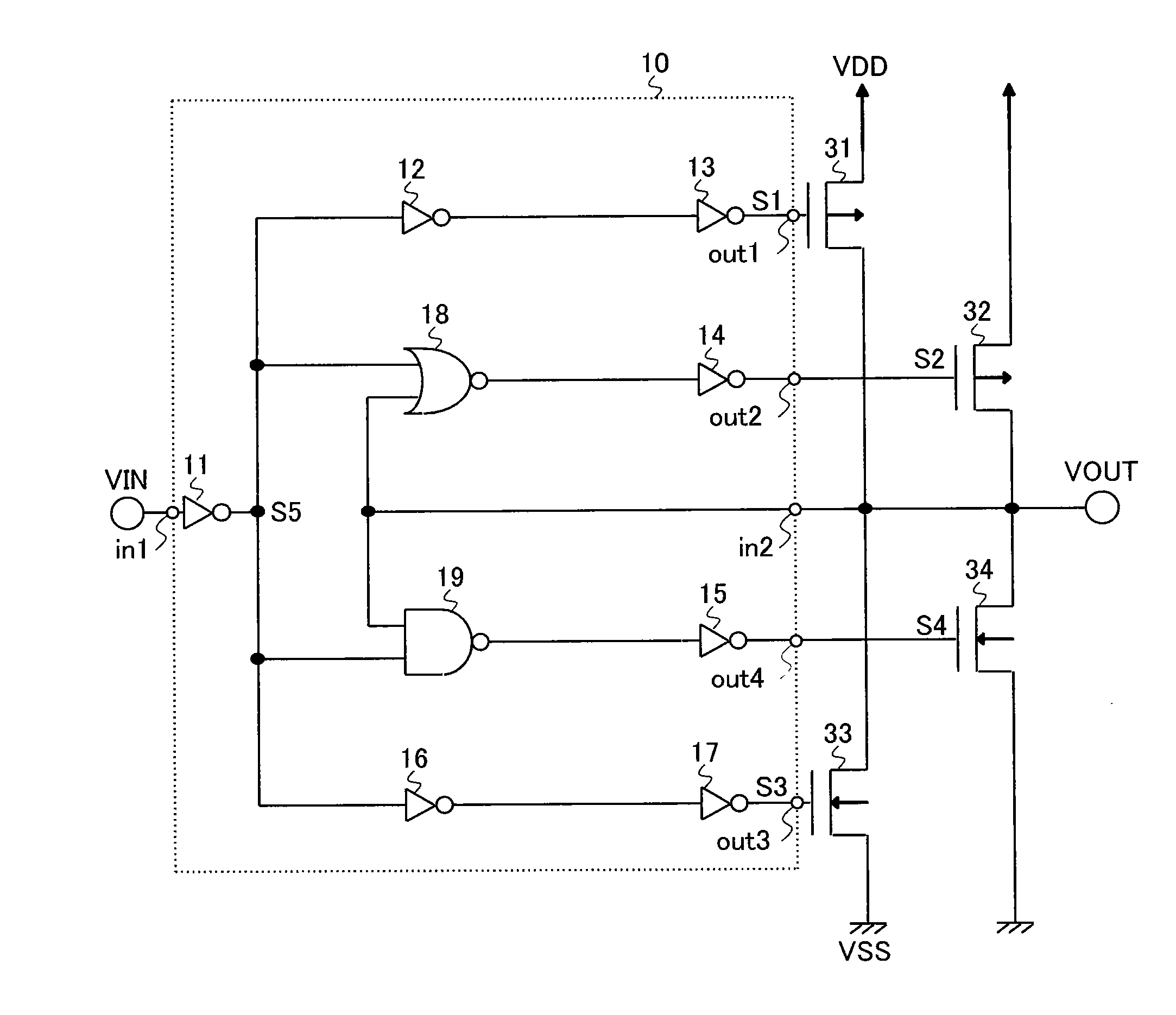
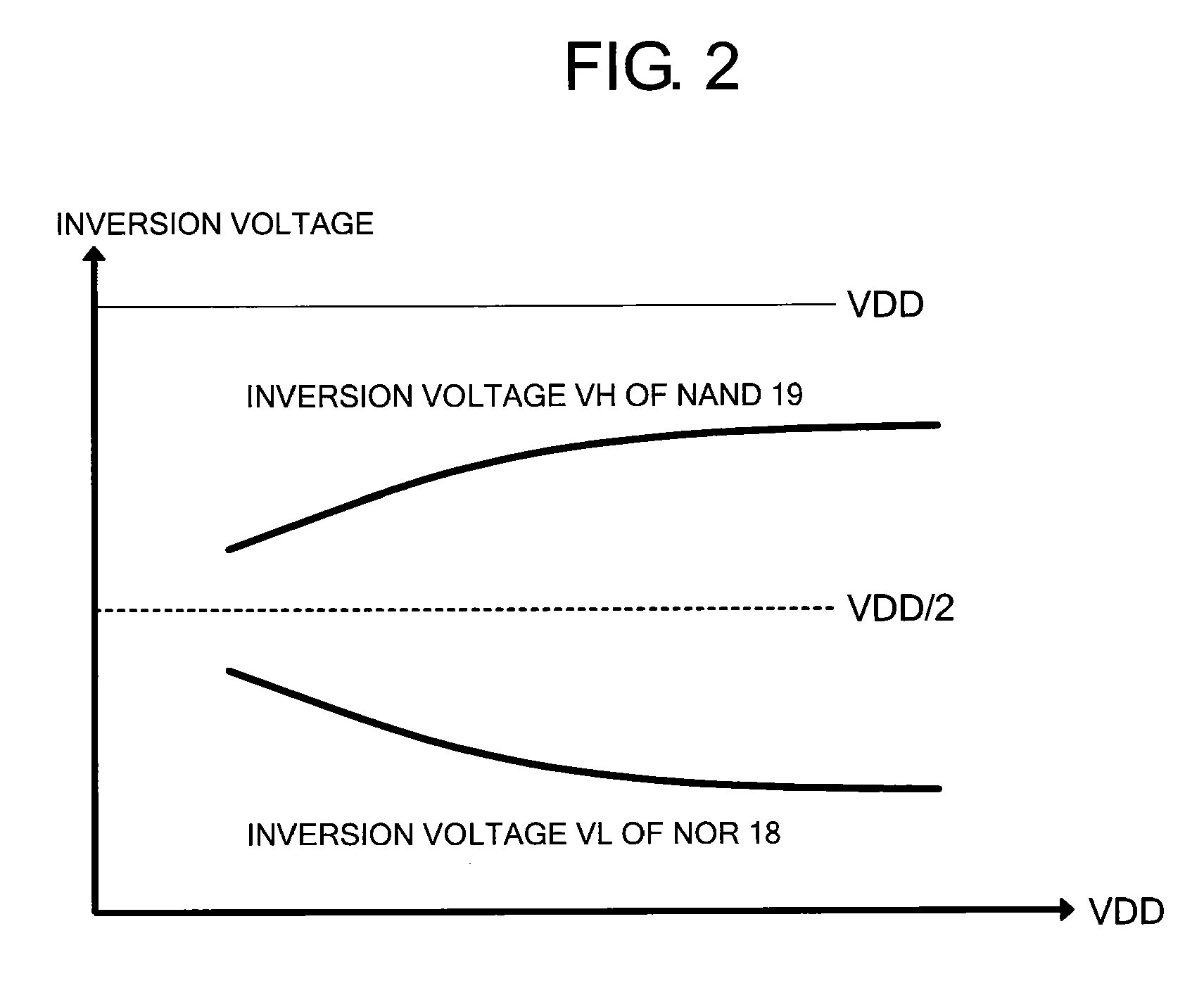
[0041]FIG. 1 is a diagram illustrating the output buffer circuit. FIG. 2 is a graph illustrating an inversion voltage.

[0042]The output buffer circuit includes a control circuit 10, PMOS transistors (PMOS) 31 and 32 that function as first transistors, and NMOS transistors (NMOS) 33 and 34 that function as second transistors.

[0043]The control circuit 10 includes inverters 11 to 17, a NOR 18, and a NAND 19. Further, a voltage input to the output buffer circuit is an input voltage VIN, a voltage output from the output buffer circuit is an output voltage VOUT, output voltages of the inverters 13 and 14, the inverter 17, and the inverter 15 are respectively voltages S1 to S4, and an output voltage of the inverter 11 is a voltage S5.

[0044]The inverters 13, 14, 15, and 17 of this embodiment function as a first logic circuit having a predetermined driving ability or less, and the NOR 18 and the NAND 19 function as a second...

second embodiment

[0086]Next, a second embodiment is described.

[0087]First, the configuration of an output buffer circuit is described.

[0088]FIG. 5 is a diagram illustrating an output buffer circuit. FIG. 6 is a diagram illustrating an inversion voltage.

[0089]The output buffer circuit includes a control circuit 40, PMOS transistors 61 and 62 that function as first transistors, and NMOS transistors 63 and 64 that function as second transistors.

[0090]The control circuit 40 has inverters 41 to 49, a NAND 51, a NAND 52, a NOR 53, and a NOR 54. Further, a voltage input to the output buffer circuit is an input voltage VIN, a voltage output from the output buffer circuit is an output voltage VOUT, output voltages of the inverter 43, the NAND 52, the inverter 49, and the NOR 54 are voltages S9 to S12, respectively.

[0091]The inverters 44 and 46 of this embodiment function as a third logic circuit.

[0092]A first input terminal in1 of the control circuit 40 is connected to an input terminal of the output buffer ...


PUM


Abstract

Provided is an output buffer circuit capable of reducing output noise, and increasing a response speed. In a case where an output voltage changes from a ground voltage to an inversion voltage of NOR, and a case where the output voltage changes from a power supply voltage to an inversion voltage of NAND, both of two MOS transistors control the output voltage, and hence, a slew rate of the output voltage becomes steep. Thus, a response speed of the output buffer circuit becomes high. Further, in such a case where the output voltage changes in the vicinity of a voltage (VDD / 2) other than the above-mentioned cases, only one MOS transistor controls the output voltage, and hence, the slew rate of the output voltage becomes gentle. Thus, a response speed of the output buffer circuit becomes low, which reduces output noise.

Description

RELATED APPLICATIONS[0001]This application claims priority under 35 U.S.C. §119 to Japanese Patent Application No. 2009-036227 filed on Feb. 19, 2009, the entire content of which is hereby incorporated by reference.BACKGROUND OF THE INVENTION[0002]1. Field of the Invention[0003]The present invention relates to an output buffer circuit that adjusts a slew rate of an output voltage of an output terminal.[0004]2. Description of the Related Art[0005]Currently, in a semiconductor integrated circuit, an output buffer circuit is used frequently for outputting an output voltage of a certain circuit to an input terminal of a circuit in a subsequent stage with desired characteristics.[0006]The output buffer circuit is required to prevent the circuit in the subsequent stage from operating incorrectly by reducing output noise.[0007]A conventional output buffer circuit is described.[0008]FIG. 8 is a diagram illustrating the conventional output buffer circuit. FIG. 9 is a timing chart illustratin...

Claims


Application Information

Patent Timeline
Patent Type & Authority Applications(United States)
IPC IPC(8): G05F1/10
CPCH03K19/01721
Inventor SATO, YUTAKA
Owner SEIKO INSTR INC
Why Eureka
Try Eureka