Scanning exposure apparatus and device manufacturing method

a technology of exposure apparatus and manufacturing method, which is applied in the direction of photomechanical apparatus, material analysis by optical means, instruments, etc., can solve the problems of inability to accurately offset correction, inability to disregarded measurement error or the effect of a surface step, and inability to ensure accuracy. , to achieve the effect of high precision offset correction and high resolution

Inactive Publication Date: 2005-11-08
CANON KK
View PDF35 Cites 4 Cited by
  • Summary
  • Abstract
  • Description
  • Claims
  • Application Information

AI Technical Summary

Benefits of technology

[0013]It is an object of the present invention to provide a surface position detecting method by which the position of a surface to be detected can be detected precisely without being affected by a surface irregularity of the surface to be detected. Particularly, it may be applied to a slit scan exposure apparatus to ensure the synchronism with respect to position, in offset control for a focus measured value, and to assure high precision offset correction for a focus measured value and a high resolution pattern transfer operation.

Problems solved by technology

Thus, such measurement error or the effect of a surface step could not be disregarded.
In such a case, unless the focus measurement point at each shot is the same as those during the offset measurement, accurate offset correction is not assured.
However, in a scan system, it is not assured.
Thus, offset correction is inaccurate.
A received light signal may be too strong and a light receiving system may be saturated.
It causes low surface position detection precision.
Thus, accurate offset correction is not attainable.
Particularly, for an electric charge accumulation type sensor, an idle reading operation due to the light adjustment operation leads to a bottle neck of a response speed during the scan operation, and the throughput is lowered or there arise insufficiency of correction points.
In a structure in which one chip is present in an exposure region, such as a case of a CPU, in the process of wafer surface clamping such as in an ion injection step or an RIE step, a photoresist remaining in a peripheral portion of the wafer may be separated and it may move to the pattern portion of the chip region, causing a pattern defect or dimension defect.
It leads to degradation of the chip yield.
Since, however, the exposure region (shot) is not rectangular as the wafer central portion, the focus measurement may end in failure and the exposure operation may be interrupted.
Even if the error is detected and processed by use of software and the exposure process is continued, there remain an increase of processing time and synchronism delay with respect to a correction system.
Thus, correction precision is not good.

Method used


Image

  • Scanning exposure apparatus and device manufacturing method
  • Scanning exposure apparatus and device manufacturing method
  • Scanning exposure apparatus and device manufacturing method

Examples


first embodiment

[First Embodiment]

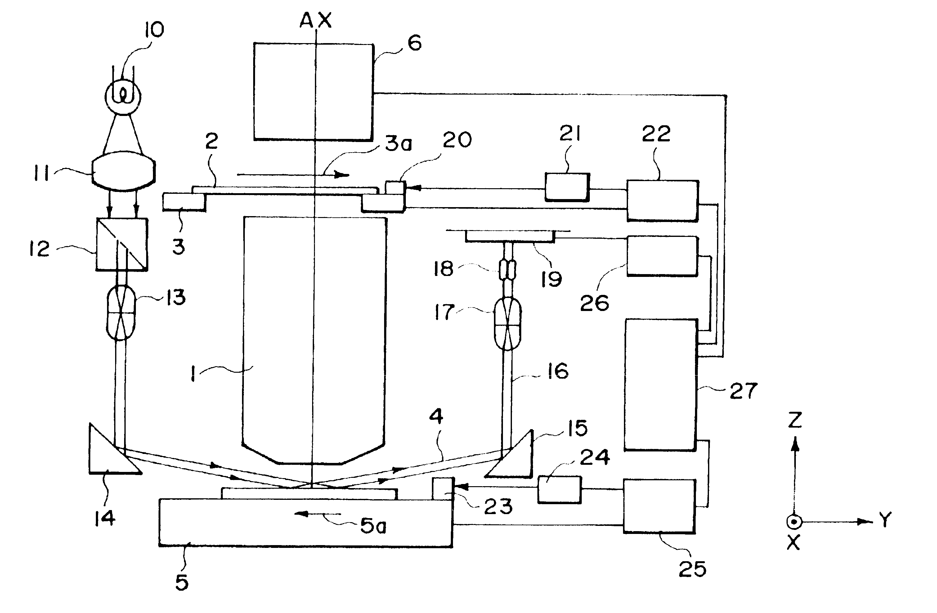
[0057]FIG. 4 is a schematic view of a main portion of a slit scan type projection exposure apparatus which uses a surface position detecting method according to a first embodiment of the present invention.

[0058]In FIG. 4, denoted at 1 is a reduction projection lens having an optical axis denoted at AX in the drawing. The image plane of it is perpendicular to the Z direction as illustrated. Reticle 2 is held by a reticle stage 3, and a pattern of the reticle 2 is projected in a reduced scale of 1:4 or 1:2 in accordance with the magnification of the reduction projection lens, whereby an image is formed on the image plane of the projection lens. Denoted at 4 is a wafer having a resist applied to its surface. There are a number of exposure regions (shots) on the wafer which are defined through a preceding exposure process or processes. Denoted at 5 is a stage on which the wafer is placed. It comprises a chuck for attracting and holding the wafer 4, an X-Y stage being m...

second embodiment

[Second Embodiment]

[0075]A slit scan type projection exposure apparatus which uses a surface position detecting method according to a second embodiment of the present invention may have the same structure as that shown in FIG. 4.

[0076]The light adjustment sequence in the surface position detecting method of this embodiment will be explained with reference to the flow chart of FIG. 10.

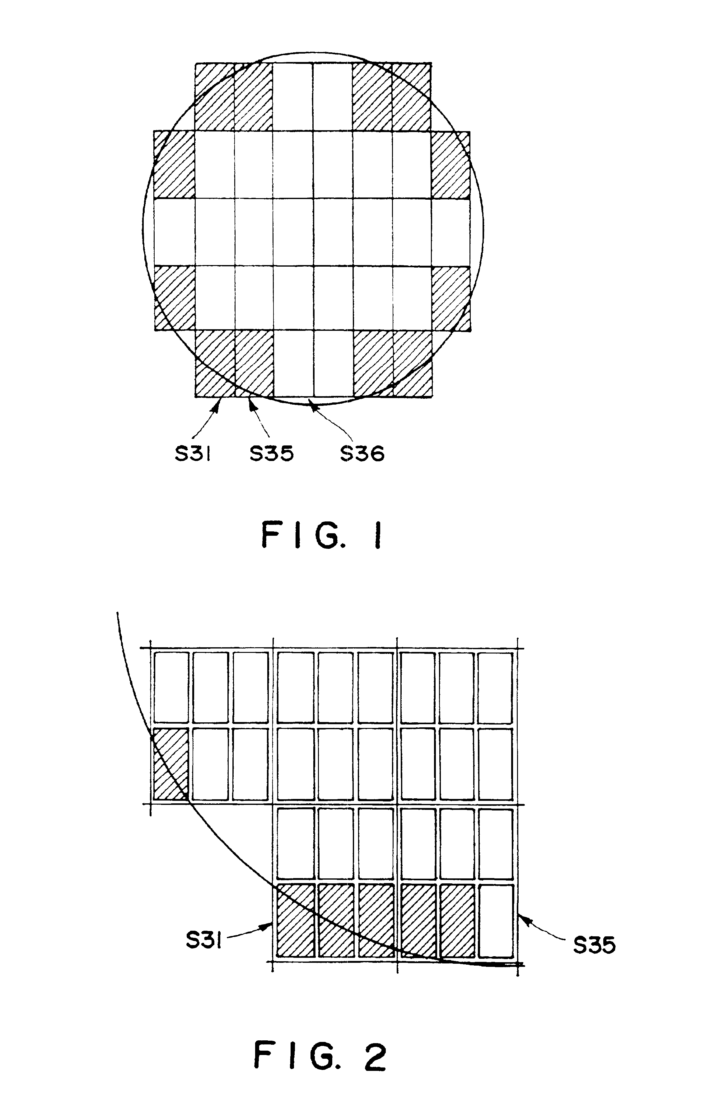
[0077]First, at step 201, measurement positions (detection points) within the shot as well as sample shots are determined on the basis of chip size, layout and exposure conditions, for example. As for the sample shots, those depicted with hatching in FIG. 7 may be selected, for example. Subsequently, at step 202, an initial value (mean) of a focus illumination light quantity is set. Then, at step 203, a wafer is loaded onto the stage and, at step 204, prealignment is performed. At step 205, focus (Z) correction is performed to the sample shot determined as above. After it, pre-scan measurement is perfor...

third embodiment

[Third Embodiment]

[0088]In a scanning exposure apparatus according to a third embodiment of the present invention, effectiveness / ineffectiveness information related to focus measurement active channels (plural measurement locations per each sensor) during the exposure operation may be determined beforehand, on the basis of wafer size, shot size, chip size, ineffectiveness range, exposure condition, for example. The focus measurement sample channels during the scan may be switched dynamically on the basis of the information, and data of height with respect to the direction (optical axis) of the projection lens, as well as tilt, may be produced.

[0089]The scan direction for each shot is set by use of effectiveness information of the focus sensor, so that the scan is made from one with a larger number of effective sensors to one with a smaller number of effective sensors. On that occasion, for a shot (e.g., rectangular portion) in which the number of effective channels is the same for a...


PUM

PropertyMeasurementUnit
sizeaaaaaaaaaa
diameteraaaaaaaaaa
depthaaaaaaaaaa

Abstract

A scanning exposure apparatus includes a surface position adjuster for adjusting the surface position of an object with respect to an image plane of a projection optical system, on the basis of a detection by the surface position detector in the projection, a controller for controlling a moving system and the surface position detector to perform a pre-scan measurement of the surface position of the object, prior to the projection, so as to detect an error, related to the detection through the surface position detector, with respect to each of detection points, which error is attributable to a difference in pattern structure at the detection points in the region, the detected error being used for correcting the adjustment by the surface position adjuster in the projection, and an initializing device for initializing the surface position detector in synchronism with the scan motion and the projection, at the position where the surface position detector has started the detection in the pre-scan measurement.

Description

[0001]This application is a divisional application of application Ser. No. 08 / 904,867, filed on Aug. 1, 1997, now U.S. Pat. No. 6,559,465.FIELD OF THE INVENTION AND RELATED ART[0002]This invention relates to a surface position detecting method for detecting level (height) or tilt of a surface of an object such as a wafer, for example, having a region with a pattern structure. More particularly, the invention is concerned with a surface position detecting method usable in a slit scan type exposure apparatus, for example, for continuously detecting position or tilt of a surface of a wafer, for example, with respect to an optical axis direction of a projection optical system of the exposure apparatus.[0003]The size of recent memory chips is increasing because of a difference between the trend of cell size or resolvable line width of an exposure apparatus and the enlargement trend of memory capacity. For a first generation of 256 M, for example, it is reported that the size is about 14×...

Claims


Application Information

Patent Timeline
Patent Type & Authority Patents(United States)
IPC IPC(8): G03F9/00G03F7/20
CPCG03F7/70358G03F9/7026
Inventor YAMADA, YUICHIUZAWA, SHIGEYUKI
Owner CANON KK
Why Eureka
Try Eureka