Light-emitting device and method of manufacturing the same

a technology of light-emitting devices and manufacturing methods, which is applied in the direction of semiconductor devices for light sources, lighting and heating apparatus, and light-emitting devices of jp, can solve the problems of deteriorating heat dissipation efficiency, inability to directly bond with the light-emitting device of the jp cannot be directly bonded by a typical solder material, so as to achieve the effect of improving heat dissipation efficiency

Inactive Publication Date: 2010-08-26
TOYODA GOSEI CO LTD
View PDF13 Cites 112 Cited by
  • Summary
  • Abstract
  • Description
  • Claims
  • Application Information

AI Technical Summary

Benefits of technology

[0007]The invention is made in view of the above-mentioned circumstances, and it is an object of the invention to provide a light-emitting device and a method of manufacturing the same, in which it is possible to improve heat dissipation efficiency without increasing the number of components and the number of manufacturing processes even when a heat dissipating member formed of aluminum, aluminum alloy, magnesium or magnesium alloy is used.
[0026]According to embodiments of the invention, it is possible to improve heat dissipation efficiency without increasing the number of components and the number of manufacturing processes even when a heat dissipating member formed of aluminum, aluminum alloy, magnesium or magnesium alloy is used.

Problems solved by technology

However, when the housing is formed of aluminum, aluminum alloy, magnesium or magnesium alloy, the light-emitting device of the JP-A 2006-5290 cannot be directly bonded by a typical solder material since an oxide film is formed on a surface of the housing.
In addition, since the oxide film formed on the surface of the housing increases thermal resistance between the heat dissipating base and the housing, heat dissipation efficiency is deteriorated.

Method used


Image

  • Light-emitting device and method of manufacturing the same
  • Light-emitting device and method of manufacturing the same
  • Light-emitting device and method of manufacturing the same

Examples


first embodiment

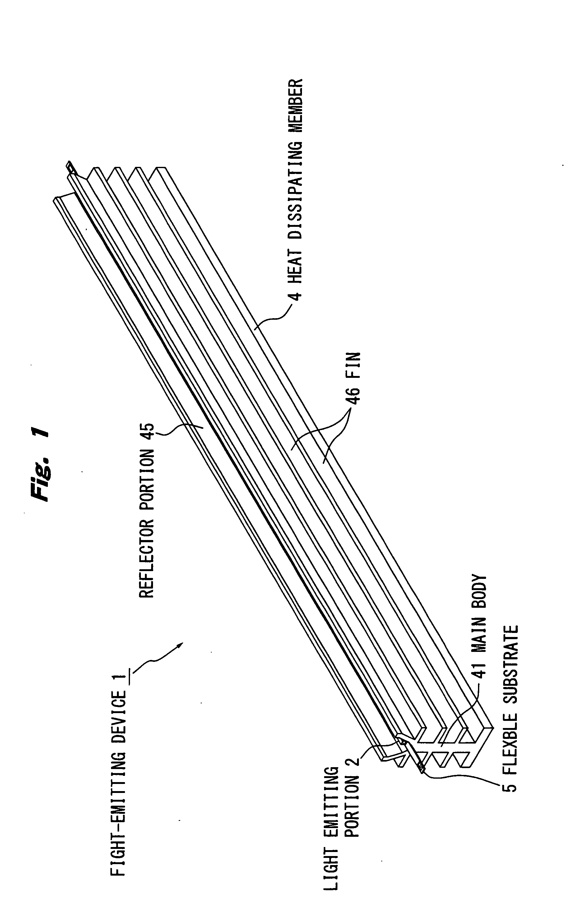
[0046]to FIGS. 1 to 4 show the invention. FIG. 1 is an outline perspective view of a light-emitting device.

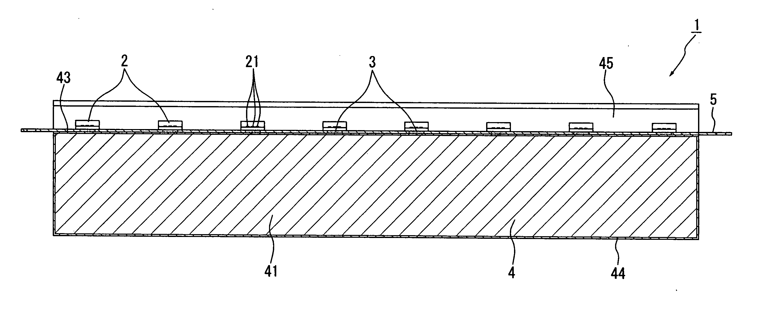
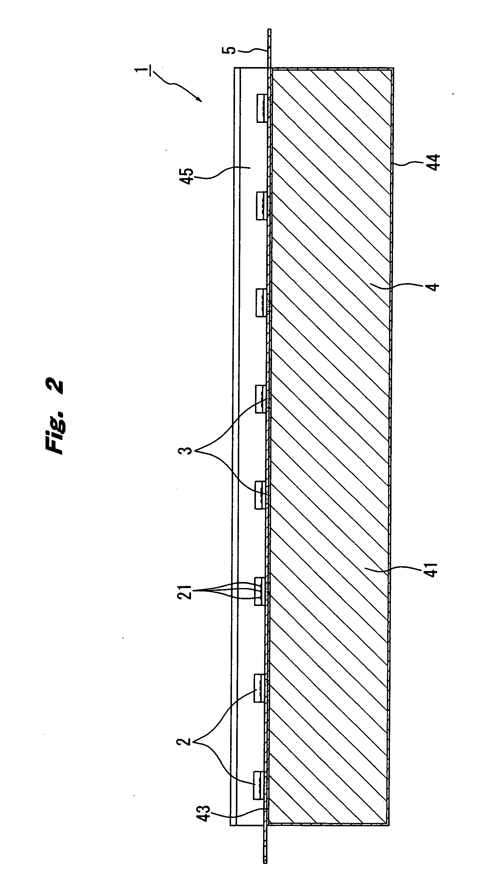
[0047]As shown in FIG. 1, a light-emitting device 1 is provided with plural light emitting portions 2 including LED elements 21, a heat dissipating member 4 connected to each light emitting portion 2 via a solder material 3 (not shown in FIG. 1), and a flexible substrate 5 for supplying power to each light emitting portion 2. The heat dissipating member 4 is formed of aluminum, and a main body 41 is formed in a plate-like shape. Each light emitting portion 2 is mounted on an upper end surface of the main body 41 of the heat dissipating member 4 at intervals. Since the heat dissipating member 4 is aluminum in which an oxide film is likely to be formed on a surface thereof, it is not possible to directly bond to the solder material 3. However, a junction 43 (not shown in FIG. 1) which is bondable to the solder material 3 is formed by performing a predetermined treatment on the he...

second embodiment

[0090]FIGS. 13 to 15 show the invention, and FIG. 13 is a lateral cross-sectional schematic diagram of the light-emitting device.

[0091]As shown in FIG. 13, a light-emitting device 101 is provided with plural light emitting portions 102 including LED elements 121, a heat dissipating member 104 connected to each light emitting portion 102 via a solder material 103, and a flexible substrate 105 for supplying power to each light emitting portion 102. The light-emitting device 101 is provided with a light guide plate 106 to which the light emitted from each light emitting portion 102 enters, and is configured such that a surface of the light guide plate 106 planarly emits light.

[0092]The heat dissipating member 104 is formed of aluminum, and is formed by extrusion. The heat dissipating member 104 has a mounting substrate 141 formed on one end side of the light guide plate 106 for mounting each light emitting portion 102 and a flange portion 145 covering another end side of the light guid...

third embodiment

[0104]FIG. 16 is a vertical cross sectional view showing a light-emitting device in the invention.

[0105]As shown in FIG. 16, a light-emitting device 201 is an indirect lighting type, which does not directly radiate the light emitted from a light emitting portion 202 outside but radiates light outside after reflecting at a reflector portion 245. The light-emitting device 201 is provided with a light emitting portion 202 including a LED element, etc., a heat dissipating member 204 connected to the light emitting portion 202 via a solder material 203, and a flexible substrate 205 for supplying power to the light emitting portion 202. In the present embodiment, the heat dissipating member 204 is a housing which houses the light emitting portion 202 and has an opening 204a formed at an upper side. The light-emitting device 201 is provided with a plate-like glass member 209 for closing the opening 204a.

[0106]The heat dissipating member 204 is formed of aluminum, and has a mounting substr...


PUM

PropertyMeasurementUnit
forward currentaaaaaaaaaa
forward voltageaaaaaaaaaa
peak wavelengthaaaaaaaaaa

Abstract

A light-emitting device includes a light emitting portion comprising a substrate having a mounting surface for mounting a LED element and a metal portion formed on a surface of the substrate opposite to the mounting surface, the substrate comprising ceramic or a semiconductor and the metal portion being bondable to a solder material and a heat dissipating member comprising aluminum, aluminum alloy, magnesium or magnesium alloy, and having, on a surface thereof, a junction treated so as to be bondable to the solder material and a heat dissipating film formed in a periphery of the junction, wherein the metal portion of the light emitting portion is bonded to the junction of the heat dissipating member by the solder material.

Description

[0001]The present application is based on Japanese Patent Application No. 2009-040765 filed on Feb. 24, 2009, the entire contents of which are incorporated herein by reference.BACKGROUND OF THE INVENTION[0002]1. Field of the Invention[0003]The invention relates to a light-emitting device having a heat dissipating member formed of aluminum, aluminum alloy, magnesium or magnesium alloy, and to a method of manufacturing the same.[0004]2. Related Art[0005]As this type of device, a light-emitting device is known which includes a high thermal conductive heat dissipating base having a mounting surface for die bonding, a circuit substrate placed on the heat dissipating base and having a hole exposing a portion of the mounting surface and a stretching portion which stretches outward from an outer peripheral edge of the heat dissipating base, a light-emitting element mounted on the mounting surface through the hole, and a translucent resin body for sealing an upper side of the light-emitting ...

Claims


Application Information

Patent Timeline
Patent Type & Authority Applications(United States)
IPC IPC(8): F21V1/00F21V19/00F21V29/00B05D5/06
CPCF21S4/008F21S48/328F21V7/005F21V29/004F21V29/763F21Y2103/003Y10S362/80F21V29/75F21V29/76F21Y2101/02F21S4/28F21Y2103/10F21Y2115/10H01L33/64F21S45/47
Inventor SUEHIRO, YOSHINOBUTASUMI, KOJI
Owner TOYODA GOSEI CO LTD
Why Eureka
Try Eureka