Manufacturing method of semiconductor device, semiconductor device, and electronic device
Inactive Publication Date: 2010-09-09
SHINKO ELECTRIC IND CO LTD
View PDF3 Cites 18 Cited by
Summary
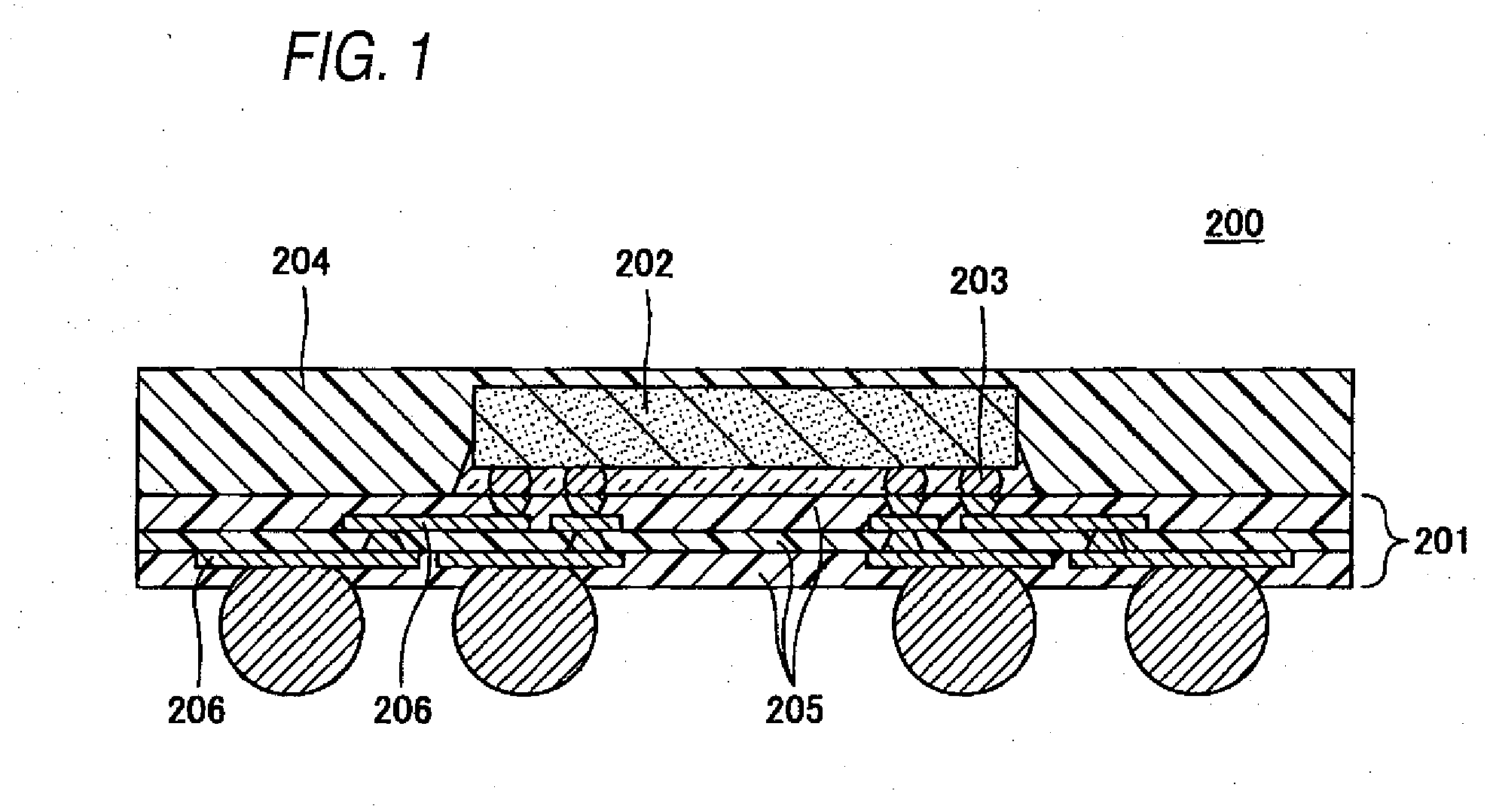
Abstract
Description
Claims
Application Information
AI Technical Summary
This helps you quickly interpret patents by identifying the three key elements:
Problems solved by technology
Method used
Benefits of technology
Benefits of technology
[0010]The present invention has been made to solve the above-described problems, and therefore, has an object to provide a manufacturing method for a semiconductor device, a semiconductor device, and an electronic device, which are capable of making wiring density of wiring layers in a very fine mode, which are provided in a wiring board, and are capable of improving electric connection reliability between a semiconductor element and the wiring board by performing the below-mentioned manufacturing method: That is, since the semiconductor element is caused to abut against wall planes of a penetration portion of a plate-shaped member, or the like, which stores thereinto the semiconductor element, an alignment of the semiconductor element is carried out in high precision by utilizing the solid wall planes, and thus, the high positional setting (alignment) precision is secured.
[0046]In accordance with the present invention, the wiring density of the wiring layers provided in the wiring board can be made in the very fine mode, and the electric connection reliability between the semiconductor element and the wiring board can be improved.
Problems solved by technology
Also, in the case that the solder bumps are employed as the bumps 203, there is a risk that a shortcircuit may occur due to migrations of the solder.
Thus, there is another problem that electric connection reliability between the wiring board 201 and the semiconductor element 202 is lowered.
Method used
Image
Click on the blue label to locate the original text in one second.
Reading with bidirectional positioning of images and text.
Examples
first embodiment
Modification 5 of First Embodiment Mode
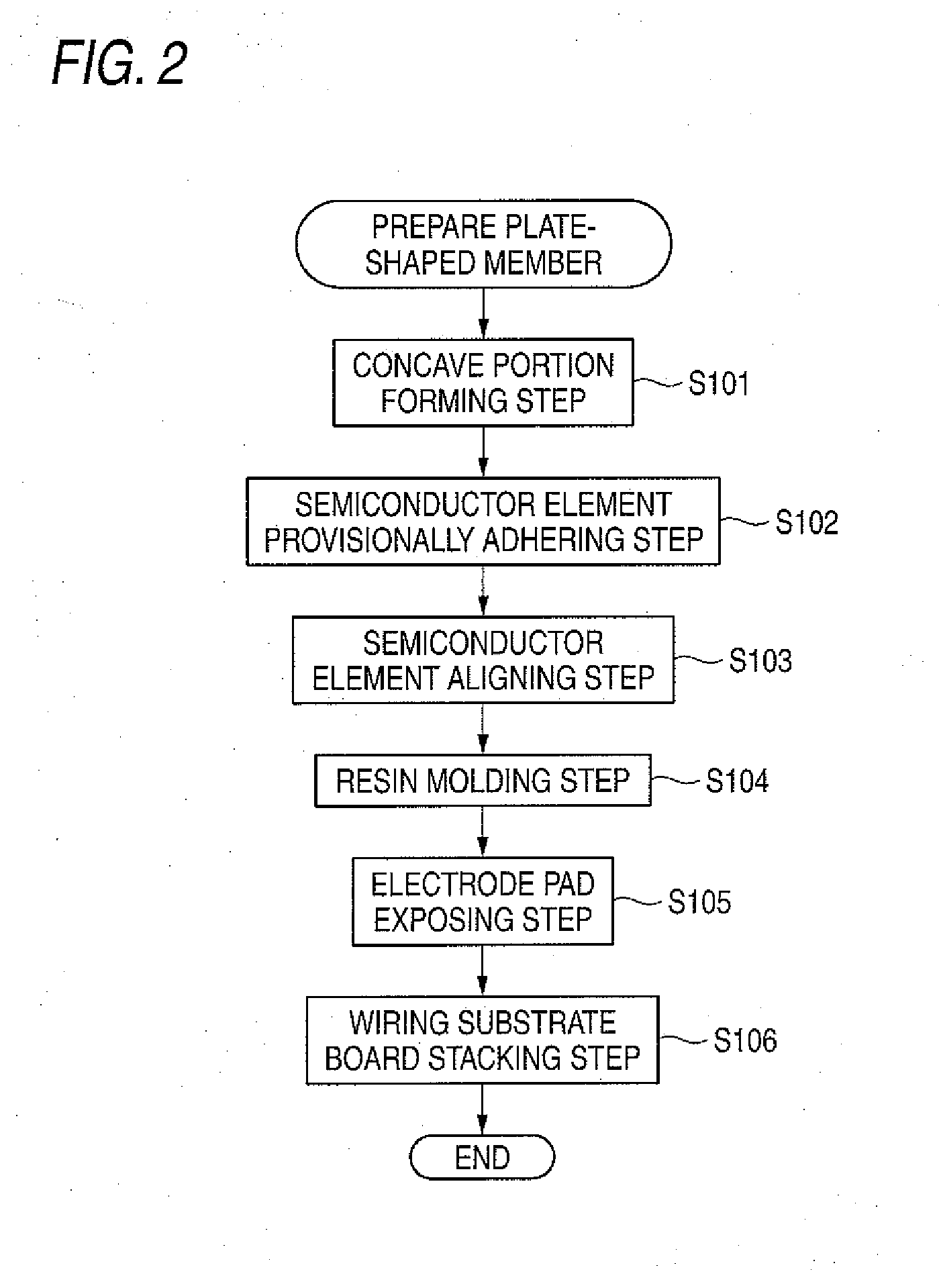
[0136]A modification 5 of the first embodiment mode is an example of a manufacturing method for a semiconductor device, which is featured by that a molded resin on a plate-shaped member is ground and polished.
[0137]FIG. 21 is a flow chart for showing steps of a manufacturing method for a semiconductor device, according to the modification 5 of the first embodiment mode. In comparison with the steps of FIG. 17, both a resin molding step (S104A) and a molded resin removing step (S105A) are different in the steps of FIG. 21.
[0138]In the resin molding step (S104A), both the semiconductor element 23 and the semiconductor element depressing member 26 stored in the concave portion 60 are sealed by employing a resin. Further, a resin is molded on a plane of the plate-shaped member 22, which is located opposite to the side of the electrode pads 27 of the semiconductor element 23 so as to provide a molded resin 25.
[0139]Next, as shown in FIG. 22, the ele...
second embodiment
Modification of Second Embodiment Mode
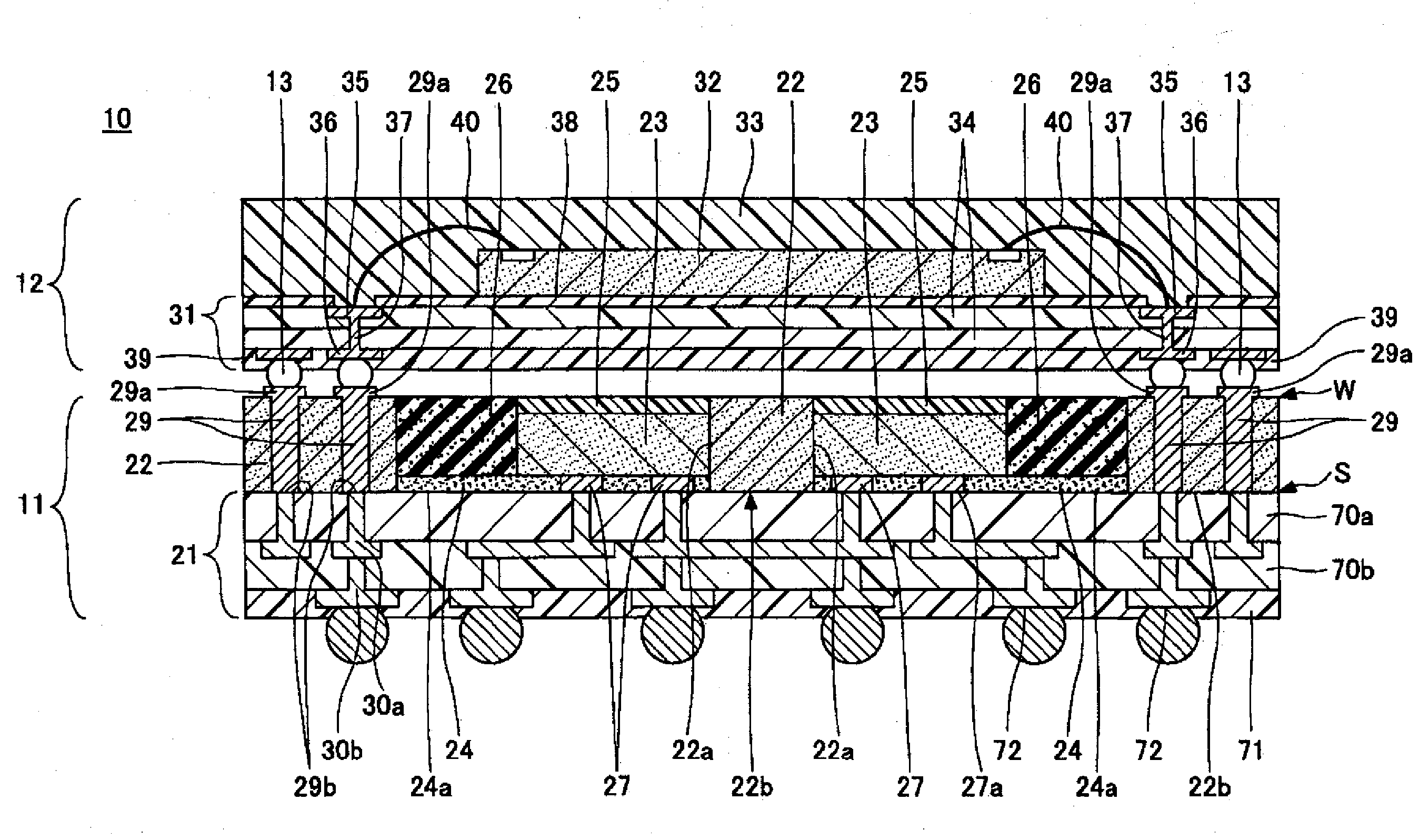
[0159]A modification of the second embodiment mode of the present invention is an example of a semiconductor device featured by that penetration electrodes are provided in a circumferential area of penetration portions of a plate-shaped member.
[0160]FIG. 25 is a sectional view for showing a semiconductor device 11 in which a wiring board 21 is stacked on a plate-shaped member 22 having penetration electrodes 29 at a circumferential area of penetration portions 22a. FIG. 26 is a plan view (being illustrated after molded resin has been removed) of the semiconductor device 11, as viewed from a second plane “W” which is located opposite to the first plane “S” of the plate-shaped member 22.
[0161]The semiconductor device 11 according to the modification of the second embodiment mode has such a different structure that penetration electrodes 29 are provided, as compared with the above-described semiconductor device 11 (FIG. 23) of the second embodiment...
[0174]In accordance with the third embodiment mode of the present invention, since the semiconductor device indicated in the above-explained second embodiment mode is used to be connected to another semiconductor device, the compact and high-density electronic device having the high reliability can be provided.
[0175]Since the above-described semiconductor device of the second embodiment mode is such a semiconductor device having a wiring board capable of achieving very fine wiring lines by employing a semiconductor element whose high alignment precision is maintained, an electronic device manufactured in high density can be provided by connecting the above-explained semiconductor device to another semiconductor device.
[0176]Also, as to the semiconductor device of the second embodiment mode, which is utilized when the electronic device of the third embodiment mode is manufactured, the higher reliability can be obtained by connecting the wiring board ...
PUM
Abstract
In a method for manufacturing a semiconductor device having a plate-shaped member, a semiconductor element, and a wiring board, the manufacturing method for the semiconductor device includes: a concave portion forming step (S101) of the plate-shaped member; a semiconductor element provisionally adhering step (S102) for provisionally adhering the semiconductor element to a portion located in the vicinity of a first corner portion of a concave portion; a semiconductor element aligning step (S103) for aligning the semiconductor element based upon thermal expansion of a semiconductor element depressing member; a resin molding step (S104) of the plate-shaped member; an electrode pad exposing step (S105) for exposing an electrode pad by grinding the plate-shaped member; and a wiring board stacking step (S106) for stacking layers by directly connecting the exposed electrode pad to the wiring layer on the ground plane of the plate-shaped member.
Description
CROSS-REFERENCE TO RELATED APPLICATION[0001]This application is based on and claims priority under 35 U.S.C. §119 from Japanese Patent Application No. 2009-048955 filed on Mar. 3, 2009.BACKGROUND OF THE INVENTION[0002]1. Technical Field[0003]The present invention is related to a method of manufacturing a semiconductor device equipped with semiconductor element and a wiring board which is electrically connected to the semiconductor element, and related to a semiconductor device and an electronic device.[0004]2. Related Art[0005]FIG. 1 is a sectional view of a conventional semiconductor device.[0006]In FIG. 1, the conventional semiconductor device 200 has a wiring board 201, a semiconductor element 202, a plurality of semiconductor element-purpose bumps 203, and a molded resin 204.[0007]The wiring board 201 has a plurality of insulating layers 205, and a plurality of wiring layers 206 provided in the plurality of insulating layers 205. The semiconductor element 202 is arranged on one ...
Claims
Application Information
Patent Timeline
Application Date:The date an application was filed.
Publication Date:The date a patent or application was officially published.
First Publication Date:The earliest publication date of a patent with the same application number.
Issue Date:Publication date of the patent grant document.
PCT Entry Date:The Entry date of PCT National Phase.
Estimated Expiry Date:The statutory expiry date of a patent right according to the Patent Law, and it is the longest term of protection that the patent right can achieve without the termination of the patent right due to other reasons(Term extension factor has been taken into account ).
Invalid Date:Actual expiry date is based on effective date or publication date of legal transaction data of invalid patent.

