Semiconductor integrated circuit

a technology of integrated circuits and semiconductors, applied in logic circuits characterized by logic functions, digital storage, instruments, etc., can solve problems such as the increase of circuit area and consumed curren

Inactive Publication Date: 2010-09-16
KK TOSHIBA
View PDF3 Cites 9 Cited by
  • Summary
  • Abstract
  • Description
  • Claims
  • Application Information

AI Technical Summary

Benefits of technology

[0008]A semiconductor integrated circuit according to an embodiment of the present invention comprises: logic circuits connected in a plurality of stages; a voltage-level inverting unit that is inserted in a signal transmis

Problems solved by technology

This causes an increase in a con

Method used


Image

  • Semiconductor integrated circuit
  • Semiconductor integrated circuit
  • Semiconductor integrated circuit

Examples


first embodiment

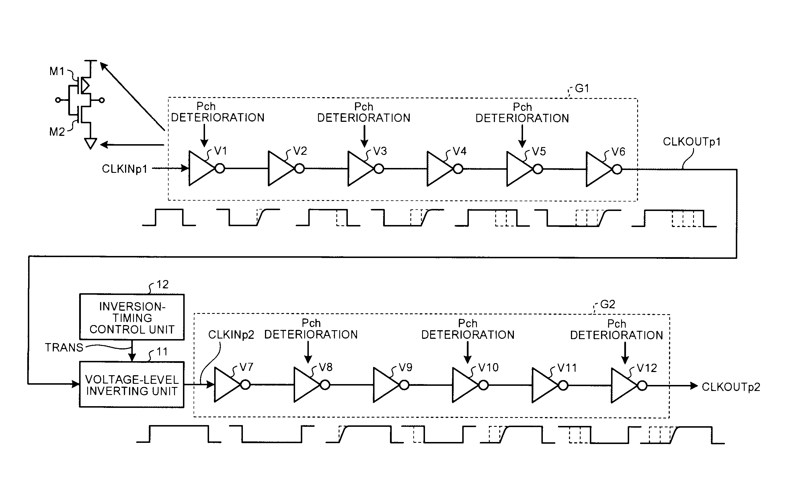
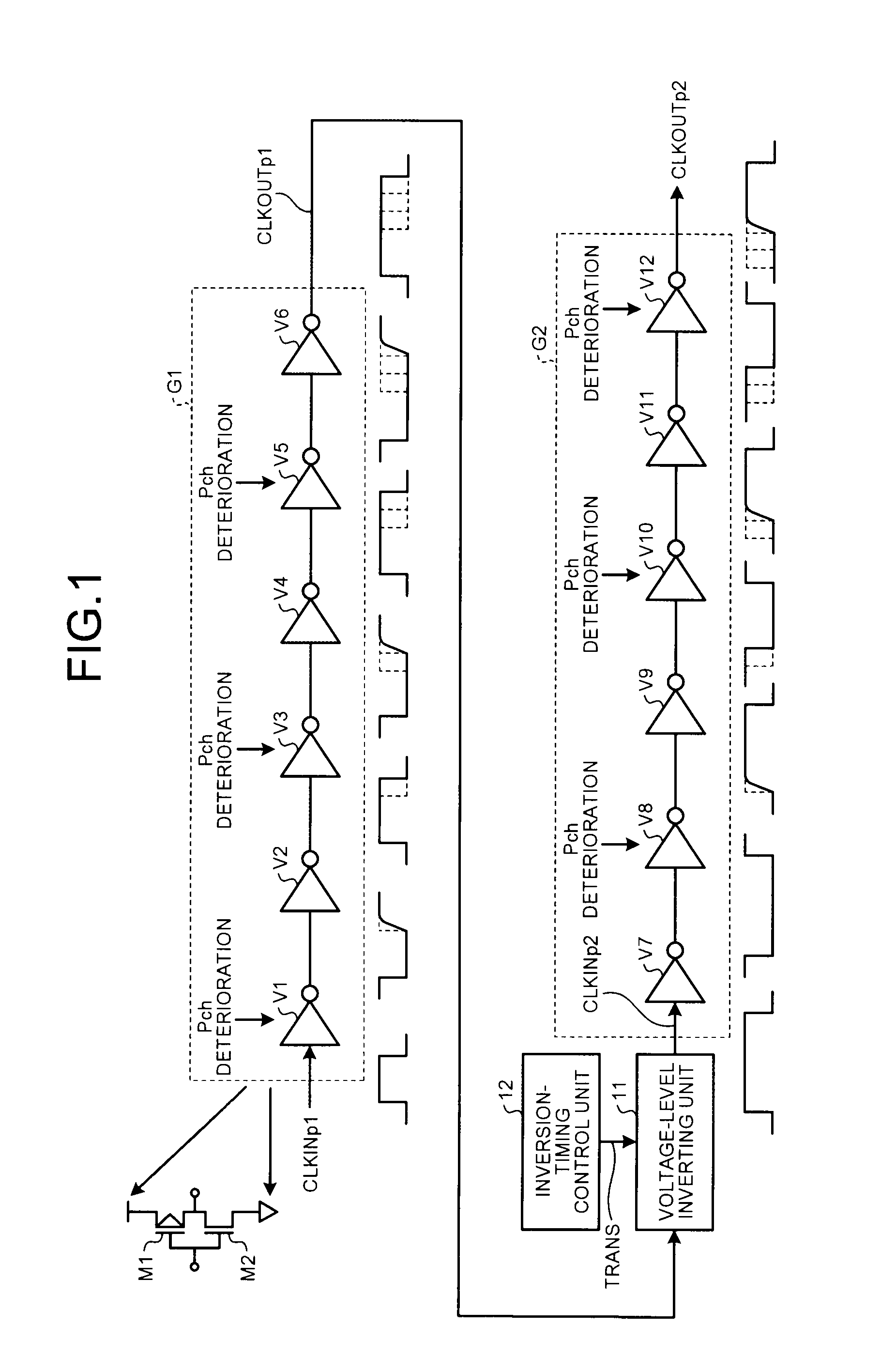
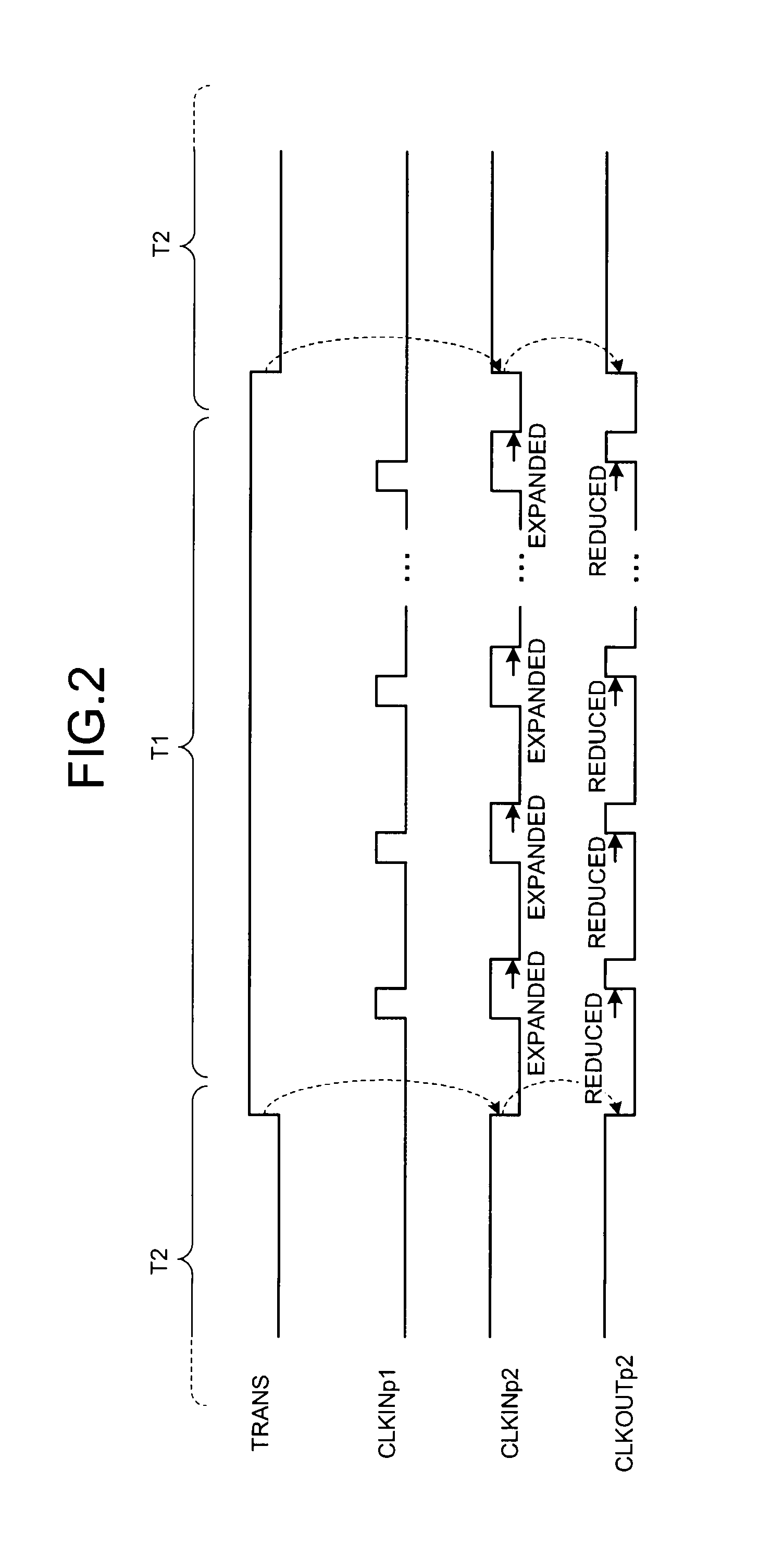
[0018]FIG. 1 is a block diagram of a schematic configuration of a semiconductor integrated circuit according to the present invention and transmission waveforms of the semiconductor integrated circuit.

[0019]In FIG. 1, the semiconductor integrated circuit includes inverters V1 to V12, a voltage-level inverting unit 11, and an inversion-timing control unit 12. The inverters V1 to V12 are connected in a plurality of stages. The inverters V1 to V12 include P-channel field effect transistors (hereinafter, “Pch transistors”) M1 and N-channel field effect transistors (hereinafter, “Nch transistors”) M2. Gates of the Pch transistors M1 and gates of the Nch transistors M2 are connected in common. Drains of the Pch transistors M1 and drains of the Nch transistors M2 are connected in common. Sources of the Pch transistors M1 are fixed at a high level (e.g., power supply potential). Sources of the Nch transistors M2 are fixed at a low level (e.g., ground potential).

[0020]The voltage-level inver...

second embodiment

[0036]FIG. 3 is a block diagram of a schematic configuration of a semiconductor integrated circuit according to the present invention.

[0037]In FIG. 3, the semiconductor integrated circuit includes shift register groups S1 and S2 and voltage-level inverting units K1 and K2. The shift register group S2 is connected to a post stage of the shift register group S1. The voltage-level inverting units K1 and K2 are respectively inserted on clock signal output sides of the shift register groups S1 and S2. The semiconductor integrated circuit also includes buffers B1 and B2 that transmit a mis-transfer prevention signal TRANS1p and buffers B3 and B4 that transmit an inversion timing control signal TRNS2p.

[0038]In a non-transmission period of a clock signal input to the shift register groups S1 and S2, the voltage-level inverting units K1 and K2 invert a voltage level input to a shift register group in the next stage. Specifically, the voltage-level inverting unit K1 includes Pch transistors ...


PUM


Abstract

A semiconductor integrated circuit includes logic circuits connected in a plurality of stages, a voltage-level inverting unit that is inserted in a signal transmission path of the logic circuits and inverts a voltage level input to the logic circuits, and an inversion-timing control unit that controls inversion timing for the voltage level inverted by the voltage-level inverting unit.

Description

CROSS-REFERENCE TO RELATED APPLICATIONS[0001]This application is based upon and claims the benefit of priority from the prior Japanese Patent Application No. 2009-060890, filed on Mar. 13, 2009; the entire contents of which are incorporated herein by reference.BACKGROUND OF THE INVENTION[0002]1. Field of the Invention[0003]The present invention relates to a semiconductor integrated circuit, and, more particularly is suitably applied to a method of suppressing a pulse waveform, which is transmitted sequentially via logic circuits including field effect transistors, from deteriorating because of negative bias temperature instability (NBTI) or positive bias temperature instability (PBTI).[0004]2. Description of the Related Art[0005]It is known that a P-channel metal-oxide semiconductor (PMOS) transistor deteriorates with time because of NBTI. The aged deterioration due to NBTI is a phenomenon in which, when an ON state of the PMOS transistor continues for a long time under a high-tempe...

Claims


Application Information

Patent Timeline
IPC IPC(8): H03K19/0175G11C19/00H03K19/20
CPCG11C19/285H03K5/15026H03K5/133H03K2005/00143H03K2005/00123
Inventor IWAI, HITOSHI
Owner KK TOSHIBA
Why Eureka
Try Eureka