
Package Level Tuning Techniques for Propagation Channels of High-Speed Signals

Inactive Publication Date: 2010-09-23
ADVANCED MICRO DEVICES INC
View PDF17 Cites 23 Cited by
  • Summary
  • Abstract
  • Description
  • Claims
  • Application Information

AI Technical Summary

Benefits of technology

[0009]In accordance with one aspect of the present invention, a method of manufacturing is provided that includes assembling a semiconductor chip carrier substrate with a first input / output site adapted to electrically connect to an external component and a second input / output site adapted to electrically connect to an input / output site of a semiconductor chip. An inductor is placed in the semiconductor chip carrier substrate. The inductor is electrically connected between the first input / output site or the second input / output site and a first conductor in the carrier substrate. The inductor has a preselected inductance to reduce an impedance discontinuity between the first input / output site or the second input / output site due to coupling to a second conductor in the semiconductor chip carrier substrate.
[0010]In accordance with another aspect of the present invention, a method of manufacturing is provided that includes forming a first conductor plane in a semiconductor chip carrier substrate. A first input / output site is formed on the semiconductor chip carrier substrate and adapted to electrically connect to an external component. A second input / output site is formed on the semiconductor chip carrier substrate and adapted to electrically connect to an input / output site of a semiconductor chip. A conductive pathway is formed between the first and second input / output sites. An inductor is formed in the semiconductor chip carrier substrate and the conductive pathway. The inductor has a preselected inductance to reduce an impedance discontinuity between the first input / output site or the second input / output site and a conductor in the carrier substrate due to coupling to the first conductor plane.
[0011]In accordance with another aspect of the present invention, an apparatus is provided that includes a semiconductor chip carrier substrate that has a first input / output site adapted to electrically connect to an external component and a second input / output site adapted to electrically connect to an input / output site of a semiconductor chip. An inductor is in the semiconductor chip carrier substrate and electrically connected between the first input / output site or the second input / output site and a first conductor in the carrier substrate. The inductor has a preselected inductance to reduce an impedance discontinuity between the first input / output site or the second input / output site and the first conductor due to coupling to a second conductor in the semiconductor chip carrier substrate.

Problems solved by technology

However, the current carrying efficiency comes with a penalty in the form of significant electrical parasitics which hamper the quality of signals propagating on the signals channels associated with the carrier substrate, particularly at higher frequencies.
Such holes can be numerous for a given conductor plane if there are many signal pins and reduce the current carrying capability of the conductor plane.
This technique presents very challenging design complexities, particularly at higher frequencies or data rates of operation.

Method used


Image

  • Package Level Tuning Techniques for Propagation Channels of High-Speed Signals
  • Package Level Tuning Techniques for Propagation Channels of High-Speed Signals
  • Package Level Tuning Techniques for Propagation Channels of High-Speed Signals

Examples


Embodiment Construction

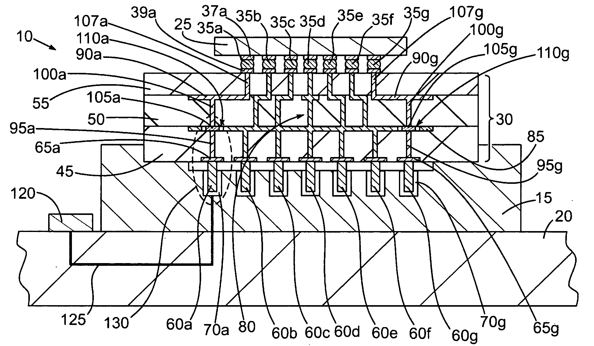
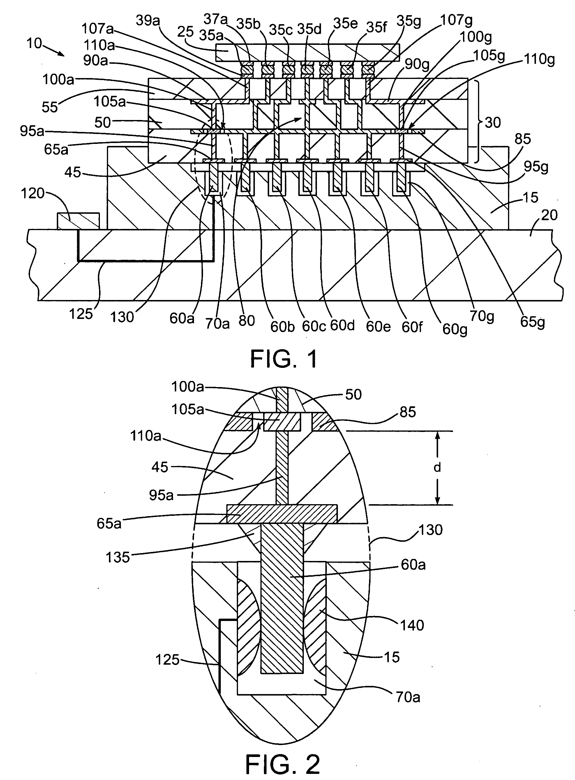
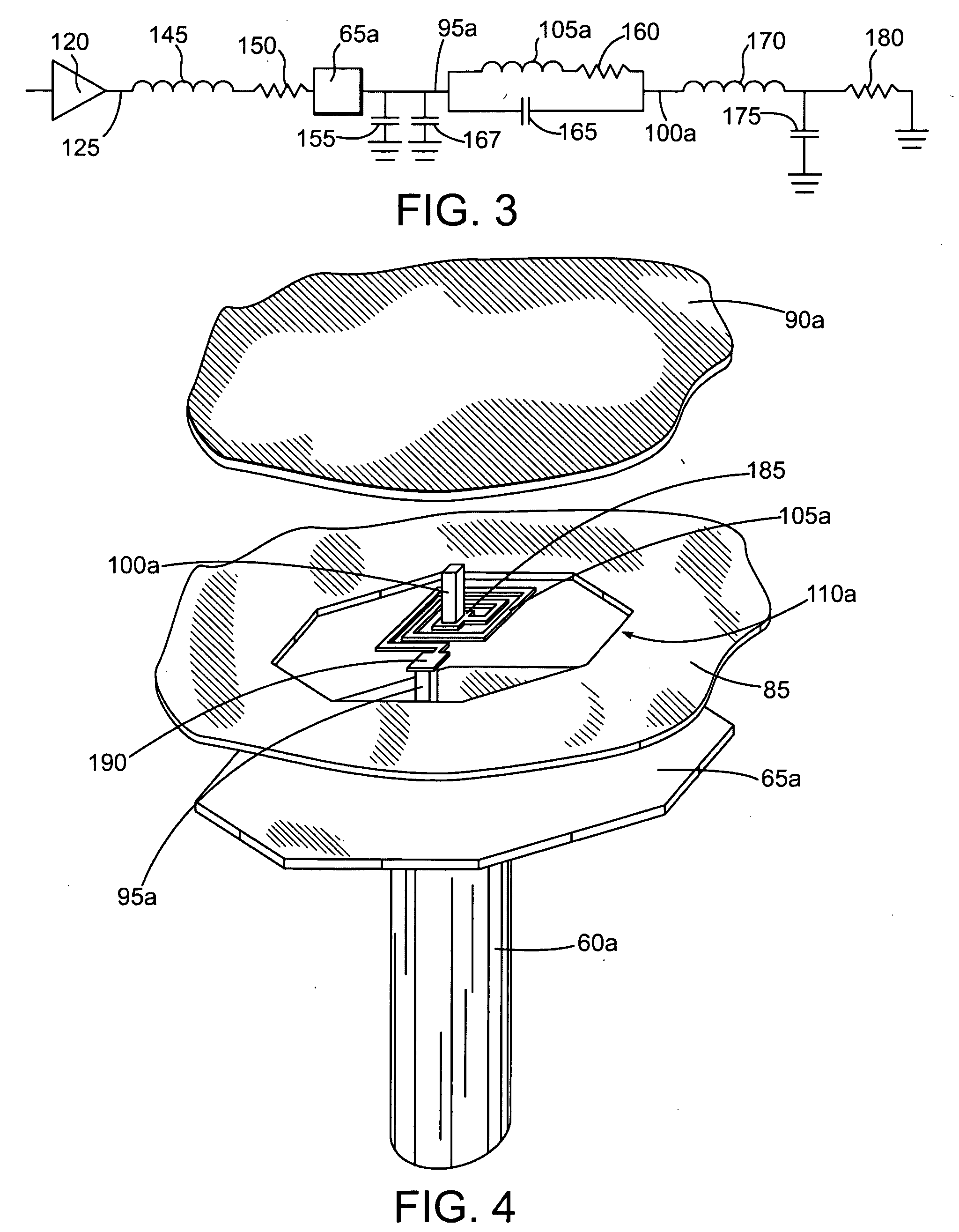
[0023]In the drawings described below, reference numerals are generally repeated where identical elements appear in more than one figure. Turning now to the drawings, and in particular to FIG. 1, therein is shown a sectional view of an exemplary embodiment of a semiconductor chip package 10 seated in a socket 15 of a printed circuit board 20. The semiconductor chip package 10 includes a semiconductor chip 25 mounted to a carrier or package substrate 30. The semiconductor chip 25 may be any of a myriad of different types of circuit devices used in electronics, such as, for example, microprocessors, graphics processors, combined microprocessor / graphics processors, application specific integrated circuits, memory devices or the like, and may be single or multi-core, or combined in a dice stack. The semiconductor chip 25 may be fabricated using silicon, germanium or other semiconductor materials. If desired, the semiconductor chip 25 may be fabricated as a semiconductor-on-insulator sub...


PUM


Abstract

Various semiconductor chip carrier substrate circuit tuning apparatus and methods are disclosed. In one aspect, a method of manufacturing is provided that includes assembling a semiconductor chip carrier substrate with a first input / output site adapted to electrically connect to an external component and a second input / output site adapted to electrically connect to an input / output site of a semiconductor chip. An inductor is placed in the semiconductor chip carrier substrate. The inductor is electrically connected between the first and second input / output sites. The inductor has a preselected inductance to reduce an impedance discontinuity between the first input / output site or the second input / output site due to coupling to a second conductor in the semiconductor chip carrier substrate.

Description

BACKGROUND OF THE INVENTION[0001]1. Field of the Invention[0002]This invention relates generally to semiconductor processing, and more particularly to apparatus and methods of reducing capacitive-based impedance discontinuity in semiconductor chip carrier substrates.[0003]2. Description of the Related Art[0004]Packaged integrated circuits often consist of one or more semiconductor chips mounted to a package or carrier substrate. The carrier substrate includes plural input / outputs designed to interface with input / outputs of a printed circuit board (PCB) of one sort or another. The input / outputs convey power, ground and signals. A typical conventional carrier substrate includes several conductor layers or planes stacked and interwoven with insulating material. Some of these planes are devoted to power and others to ground. Still other conductor pathways in the carrier substrate are slated for signals.[0005]A typical signal propagation channel consists of a PCB, a PCB socket, and a car...

Claims


Application Information

Patent Timeline
IPC IPC(8): H01L27/02H01L21/52H01L21/02H01L23/00
CPCH01L23/49811H01L23/49822H01L23/49827H01L23/645H01L2224/16225H01L2224/16235H01L2924/01078H01L2924/01079H01L2924/15312H01L2924/3011H05K1/165H01L2924/01046H01L2224/05573H01L2224/05568H01L2224/05639H01L2224/05644H01L2224/05647H01L2224/05664H01L2224/05669H01L2224/05624H01L2224/0568H01L2924/00014H01L2224/0554H01L2924/013H01L2224/05599H01L2224/0555H01L2224/0556
Inventor BEKER, BENJAMINFOPPIANO, JAMES
Owner ADVANCED MICRO DEVICES INC
Learn More