Scanner, electro-optical panel, electro-optical display device and electronic apparatus

a technology of display device and scanner, applied in the direction of static indicating device, pictoral communication, instruments, etc., can solve the problems of reducing the reliability of scanner, weakening the technique concerned against variations in manufacturing process, and destroying elements, so as to prevent the reliability and yield of scanners from being affected, the drive capability can be ensured, and the circuit area can be reduced.

Active Publication Date: 2010-09-23
JAPAN DISPLAY WEST
View PDF4 Cites 5 Cited by
  • Summary
  • Abstract
  • Description
  • Claims
  • Application Information

AI Technical Summary

Benefits of technology

[0009]With such a configuration, the bootstrap potential applied to the gate electrode of the output transistor rises sufficiently, and the drive capability can be ensured. The potential of the other end of the voltage limiting transistor is limited to the first power supply potential. Accordingly, the potentials applied to the elements (to be more specific, the above-described cutoff transistor, control transistor and reset transistor) which constitute each circuit can be limited, preventing the reliability and yield of the scanner from being affected. Moreover, the capacitor for dropping the bootstrap potential is unnecessary, and accordingly, the circuit area can also be reduced.
[0010]An advantage of another aspect of the invention is to propose: an electro-optical panel in which such a scanner is formed as a scan line drive circuit on a substrate; and an electro-optical display device and an electronic apparatus, each using the electro-optical panel. It is possible to realize a display device and an electronic apparatus, in which display quality is high since a sufficient capability is provided in the scan line drive circuit, and cost and size are suppressed.

Problems solved by technology

However, a too high bootstrap potential leads to element destruction and reliability decrease in the scanner.
In a technique for adjusting the bootstrap potential by such capacitor division as proposed in JP-A-2008-287134, a circuit area is increased owing to an element area of capacitors, and in addition, the technique concerned is weak against variations in manufacturing process.
Accordingly, the potentials applied to the elements (to be more specific, the above-described cutoff transistor, control transistor and reset transistor) which constitute each circuit can be limited, preventing the reliability and yield of the scanner from being affected.

Method used


Image

  • Scanner, electro-optical panel, electro-optical display device and electronic apparatus
  • Scanner, electro-optical panel, electro-optical display device and electronic apparatus
  • Scanner, electro-optical panel, electro-optical display device and electronic apparatus

Examples


embodiments

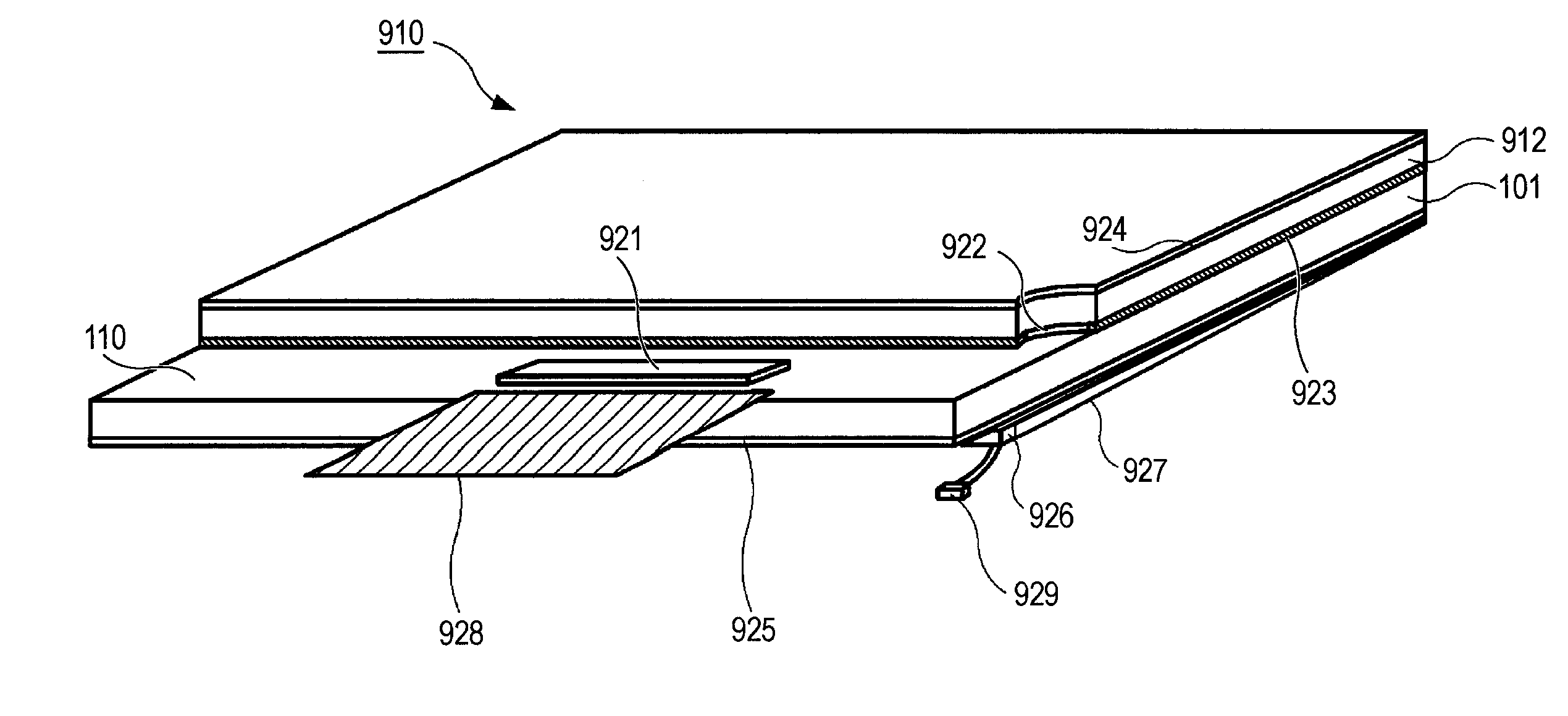
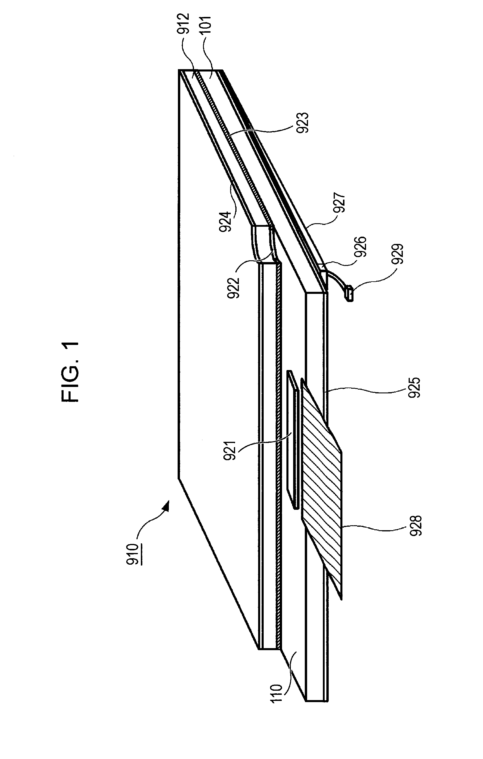
[0024]FIG. 1 is a (partially cross-sectional) perspective view of a liquid crystal display device 910 as an electro-optical panel according to an embodiment of the invention. The liquid crystal display device 910 is formed in such a manner that an active matrix substrate 101 as an active matrix device and an opposite substrate 912 are bonded to each other by a seal member 923 so as to be spaced from each other at a fixed interval, and that a nematic-phase liquid crystal material 922 is sandwiched therebetween. On the active matrix substrate 101, though not illustrated, an alignment material made of polyimide or the like is coated, and is subjected to rubbing treatment, whereby an alignment film is formed. On the opposite substrate 912, though not illustrated, color filters and a black matrix are formed. The color filters correspond to pixels, and the black matrix is made of resin with low reflectivity and low transmissibility, which is prepared for preventing light leakage and enhan...


PUM


Abstract

A scanner includes a plurality of unit circuits configured with transistors of a same conductivity type. In the scanner, the unit circuit constituting the scanner includes an output transistor that selectively outputs, to an output terminal of the unit circuit, a signal given from an outside. A gate electrode of the output transistor is connected to one end of a voltage limiting transistor, and a gate electrode of the voltage limiting transistor is supplied with a first power supply potential.

Description

BACKGROUND[0001]1. Technical Field[0002]The present invention relates to a scanner, an electro-optical panel, an electro-optical display device including the electro-optical panel, and an electronic apparatus including the electro-optical display device.[0003]2. Related Art[0004]For reducing cost of an electro-optical panel using an active matrix device, there has been known a technique of providing a drive circuit on the same substrate as that of the active matrix device. In particular, if the drive circuit is configured only with transistors of the same conductivity type that is either an n-type or a p-type, then an effect of reducing the cost of the electro-optical panel is increased. In this case, a configuration with a scanner using a bootstrap as a scan line drive circuit is typically proposed in order to sufficiently obtain a potential amplitude of an output signal of the drive circuit, and many similar configurations have been proposed. Japanese Patent No. 3658349 is an exam...

Claims


Application Information

Patent Timeline
Patent Type & Authority Applications(United States)
IPC IPC(8): G09G3/30H04N1/04
CPCG09G3/3677
Inventor KOBASHI, YUTAKA
Owner JAPAN DISPLAY WEST
Why Eureka
Try Eureka