Pattern generating method, method of manufacturing semiconductor device, and computer program product

a technology of semiconductor devices and generating methods, applied in adaptive control, process and machine control, instruments, etc., can solve the problems of reducing the wavelength of light sources, unable to meet the request for microminiaturization of semiconductor devices that advances with increasing speed, and extreme difficulty in improving yield

Inactive Publication Date: 2010-09-23
KK TOSHIBA
View PDF12 Cites 22 Cited by
  • Summary
  • Abstract
  • Description
  • Claims
  • Application Information

AI Technical Summary

Benefits of technology

[0008]A pattern generating method according to an embodiment of the present invention comprises: preparing design layout data of a semiconductor integrated circuit pattern; performing pattern formation simulations based on the design layout data subjected to OPC processing with a plurality of process parameters set in process conditions in a predetermined range; calculating, as a worst condition, based on risk points having likelihood of causing a pattern formation failure higher than a predetermined value, a process condition having a process parameter that brings about a worst result when pattern formation is performed among the process parameters, the risk point being extracted from simulation results of the pattern formation simulations; and changing the design layout data or the OPC processing such that when a pattern is formed under the worst condition based on the changed design layout data or the changed OPC processing a number of the risk points or a risk degree of the risk points of the pattern is smaller than the simulation result.
[0009]A method of manufacturing a semiconductor device according to an embodiment of the present invention comprises: preparing design layout data of a semiconductor integrated circuit pattern; performing pattern formation simulations based on the design layout data subjected to OPC processing with a plurality of process parameters set in process conditions in a predetermined range; calculating, as a worst condition, based on risk points having likelihood of causing a pattern formation failure higher than a predetermined value, a process condition having a process parameter that brings about a worst result when pattern formation is performed among the process parameters, the risk point being extracted from simulation results of the pattern formation simulations; changing the design layout data or the OPC processing such that when a pattern is formed under the worst condition based on the changed design layout data or the changed OPC processing a number of the risk points or a risk degree of the risk points of the pattern is smaller than the simulation result and forming a pattern on a wafer based on the changed design layout data or the changed OPC processing.
[0010]A computer program product executable by a computer and having a computer readable recording medium includes a plurality of commands for determining a pattern according to an embodiment of the present invention, wherein the commands cause the computer to execute: preparing design layout data of a semiconductor integrated circuit pattern; extracting risk points having likelihood of causing a pattern formation failure higher than a predetermined value from a result obtained by executing pattern formation simulations on the design layout data subjected to OPC processing using process conditions in which a plurality of parameters are set in a predetermined range; calculating, as a worst condition, based on the extracted risk points, a process condition having a process parameter that brings about a worst result when pattern formation is performed among the process parameters; and changing the design layout data or the OPC processing such that when a pattern is formed under the worst condition based on the changed design layout data or the changed OPC processing a number of the risk points or a risk degree of the risk points of the pattern is smaller than the simulation result.

Problems solved by technology

According to the microminiaturization of semiconductor devices in recent years, defects due to manufacturing fluctuation, particles, and the like increase to make it extremely difficult to improve yield.
However, the method of reducing wavelength of a light source, the method of increasing a numerical aperture of a lens, and the like cannot meet the request for microminiaturization of semiconductor devices that advances with increasing speed.
It is also likely that a new risk point occurs because of processing fluctuation during mass production.

Method used


Image

  • Pattern generating method, method of manufacturing semiconductor device, and computer program product
  • Pattern generating method, method of manufacturing semiconductor device, and computer program product
  • Pattern generating method, method of manufacturing semiconductor device, and computer program product

Examples


first embodiment

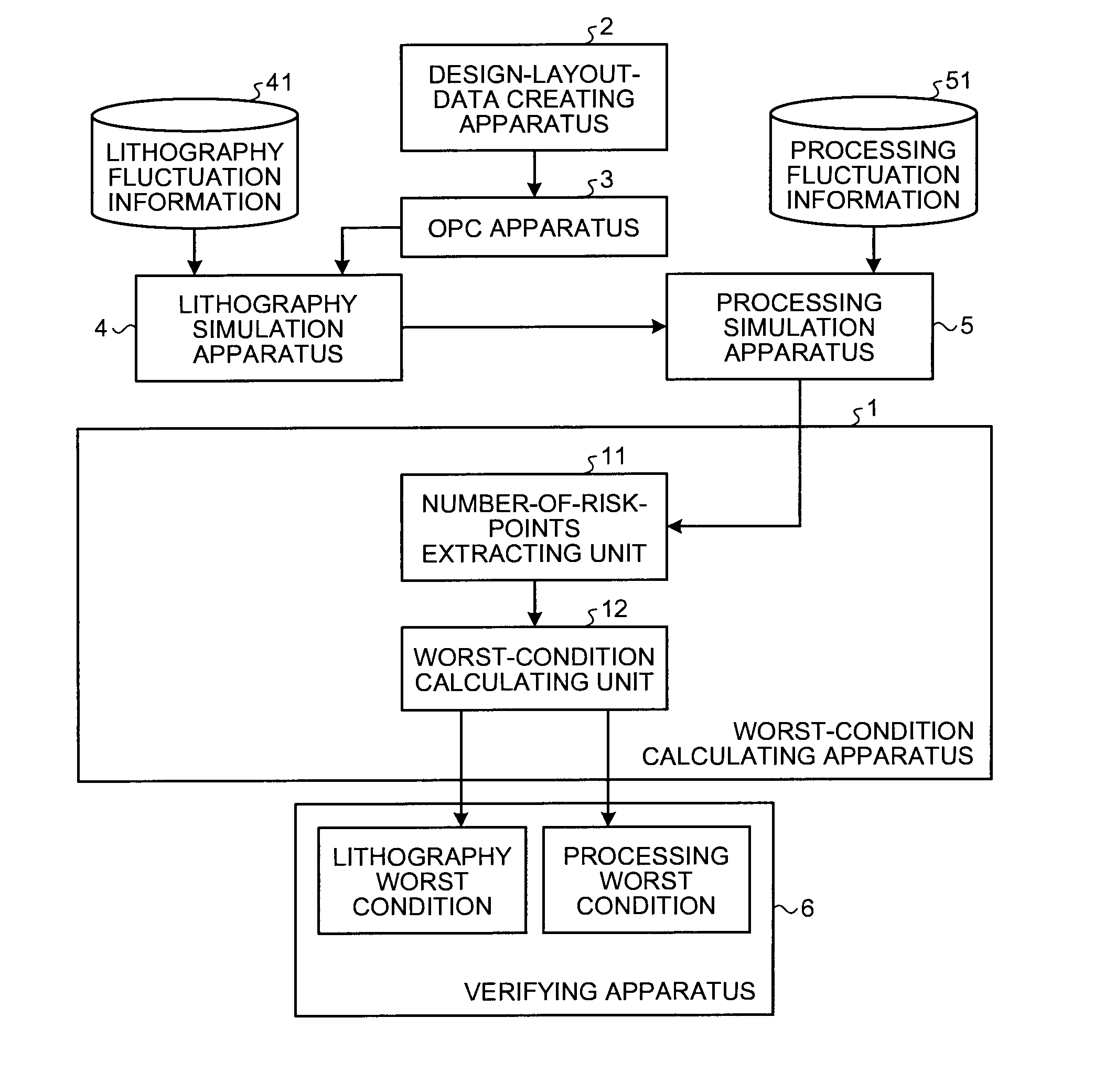
[0024]FIG. 1 is a block diagram of the configuration of a pattern forming system including a worst-condition calculating apparatus according to the present invention. The pattern forming system is a system configured to generate mask data used in forming a semiconductor integrated circuit pattern and forming patterns on a substrate such as a wafer using a mask manufactured by using the mask data. The pattern generating system generates mask data for forming patterns by processing, at least once, a film to be processed.

[0025]The pattern forming system according to this embodiment performs a lithography simulation and a processing simulation taking into account fluctuation in lithography and fluctuation in processing to thereby simulatively generate patterns formed on a substrate. The pattern forming system calculates, based on the simulatively-generated pattern, worst process conditions (a worst lithography condition and a worst processing condition). In this embodiment, to reduce th...

second embodiment

[0090]In the present invention, it is determined based on a difference (a CD difference) between a pattern dimension of simulatively-generated patterns and a best dimension whether patterns formed on a substrate are within a desired dimension range. When the patterns are not within the desired dimension range, design layout data, OPC, process conditions, and the like are changed to form patterns on the substrate. The best dimension in this embodiment is a pattern dimension (an ideal value) of patterns formed under a best condition.

[0091]FIG. 9 is a block diagram of the configuration of a pattern forming system including a CD-difference calculating apparatus according to the second embodiment. Among components shown in FIG. 9, components that attain functions same as those of the pattern forming system according to the first embodiment shown in FIG. 1 are denoted by the same reference numerals and redundant explanation of the components is omitted.

[0092]The pattern forming system acc...


PUM

PropertyMeasurementUnit
luminance distributionaaaaaaaaaa
processing fluctuationaaaaaaaaaa
processingaaaaaaaaaa

Abstract

Pattern formation simulations are performed based on design layout data subjected to OPC processing with a plurality of process parameters set in process conditions. A worst condition of the process conditions is calculated based on risk points extracted from simulation results. The design layout data or the OPC processing is changed such that when a pattern is formed under the worst condition based on the changed design layout data or the changed OPC processing a number of the risk points or a risk degree of the risk points of the pattern is smaller than the simulation result.

Description

CROSS-REFERENCE TO RELATED APPLICATIONS[0001]This application is based upon and claims the benefit of priority from the prior Japanese Patent Application No. 2009-070976, filed on Mar. 23, 2009; the entire contents of which are incorporated herein by reference.BACKGROUND OF THE INVENTION[0002]1. Field of the Invention[0003]The present invention relates to a pattern generating method, a method of manufacturing a semiconductor device, and a computer program product.[0004]2. Description of the Related Art[0005]According to the microminiaturization of semiconductor devices in recent years, defects due to manufacturing fluctuation, particles, and the like increase to make it extremely difficult to improve yield. As a method of microminiaturizing semiconductor devices, for example, there are a method of reducing wavelength of a light source (an exposure beam) and a method of increasing a numerical aperture (NA) of a lens. However, the method of reducing wavelength of a light source, the m...

Claims


Application Information

Patent Timeline
Patent Type & Authority Applications(United States)
IPC IPC(8): G05B13/04G06F17/50G03F1/36G03F1/68G03F1/70G06F19/00H01L21/027
CPCG03F1/36G03F1/144
Inventor TAGUCHI, TAKAFUMIKOTANI, TOSHIYATAKIMOTO, MICHIYANAKAJIMA, FUMIHARUABURADA, RYOTAMASHITA, HIROMITSUIYANAGI, KATSUMIKODAMA, CHIKAAKI
Owner KK TOSHIBA
Why Eureka
Try Eureka