

Light Absorbing Layer Of CIGS Solar Cell And Method For Fabricating The Same
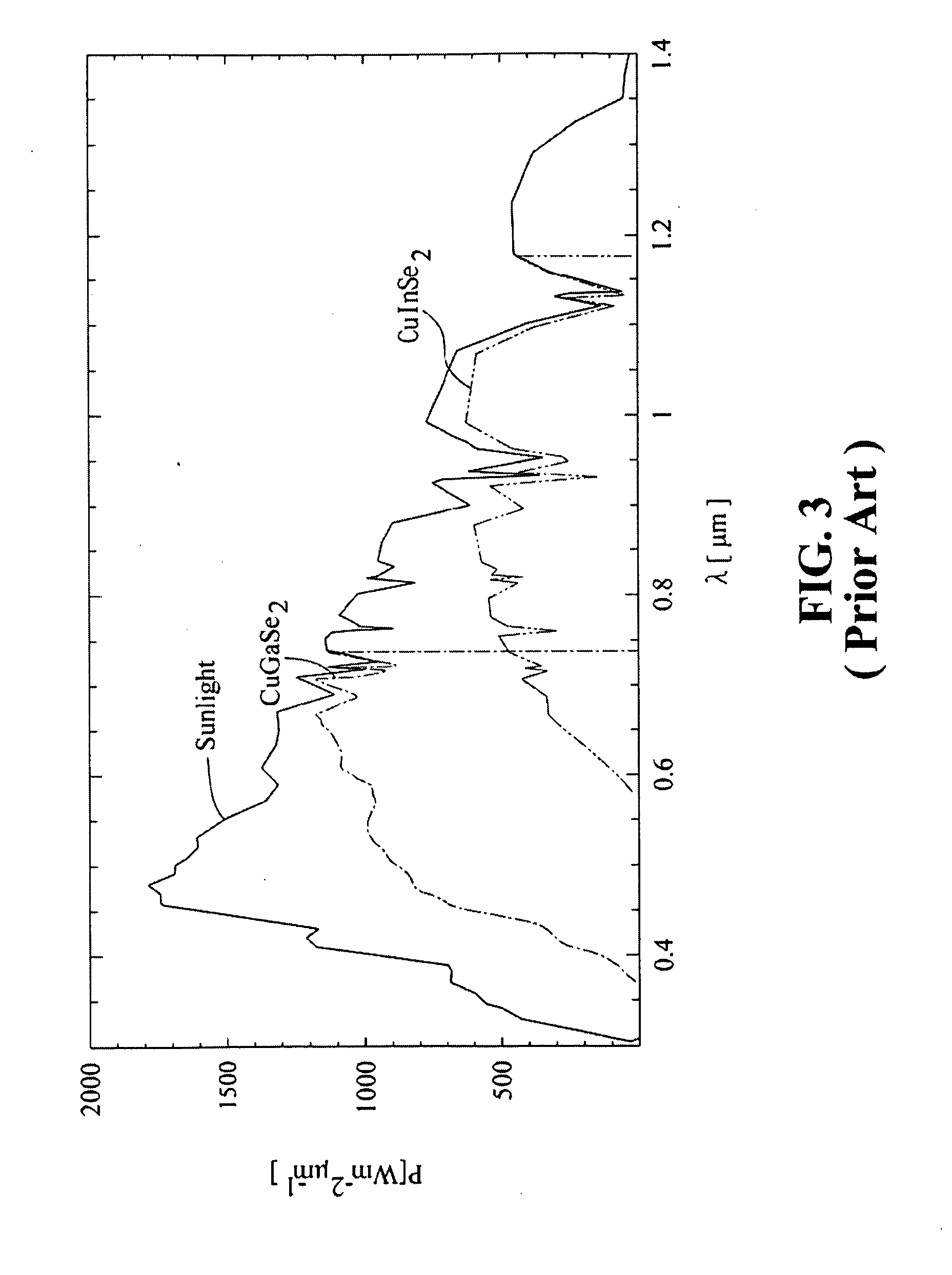
a solar cell and light absorbing technology, applied in the field of copper indium gallium diselenide (cigs) solar cells, can solve the problems of not being able to compare solar energy taken from sunlight radiation, non-renewable consumption, and mined fossil fuel sources, etc., to improve photoelectric transformation efficiency, light absorbance, and the effect of improving the efficiency of photoelectric transformation
- Summary
- Abstract
- Description
- Claims
- Application Information
AI Technical Summary
Benefits of technology
Problems solved by technology
Method used
Image

Examples
first embodiment
[0031]FIG. 4 is a schematic diagram illustrating a structure of the present invention. Referring to FIG. 4, a copper / indium / gallium / selenium (CIGS) solar cell 3 is shown. The CIGS solar cell 3 includes a glass substrate 10, a molybdenum (Mo) thin film layer serving as a back electrode layer 20, a Mo / Cu / Al / Ag alloy layer 22, a cuprous sulfide layer 24, a first mixture layer 41, a second mixer layer 42, a third mixer layer 43, and a buffer layer 80 sequentially stacked one on another from bottom to top. Specifically, the back electrode layer 20 and the Mo / Cu / Al / Ag alloy layer 22 are sequentially deposited onto the glass substrate 10. Thereafter, the cuprous sulfide layer 24, the first mixture layer 41, the second mixer layer 42, and the third mixer layer 43 are then sequentially stacked onto the Mo / Cu / Al / Ag alloy layer 22. A thermal treatment is conducted to the cuprous sulfide layer 24, the first mixture layer 41, the second mixer layer 42, and the third mixer layer 43 to form a copp...
second embodiment
[0038]FIG. 9 is a schematic diagram illustrating a structure of the present invention. Referring to FIG. 9, a CIGS solar cell 4 is shown. The CIGS solar cell 4 includes a glass substrate 10, a molybdenum (Mo) thin film layer serving as a back electrode layer 20, a Mo / Cu / Al / Ag alloy layer 22, a cuprous sulfide layer 24, a cuprous selenide layer 51, an indium selenide layer 52, a gallium selenide layer 52, and a buffer layer 80 sequentially stacked one on another from bottom to top. Specifically, the cuprous sulfide layer 24, the cuprous selenide layer 51, the indium selenide layer 52, and the gallium selenide layer 53 are sequentially stacked onto the Mo / Cu / Al / Ag alloy layer 22, and followed by a thermal treatment so that the cuprous sulfide layer 24, the cuprous selenide layer 51, the indium selenide layer 52, and the gallium selenide layer 53 are molten and mutually diffused to form a copper / indium / gallium / sulfur / selenium (CIGSS) light absorbing layer having a high light absorbance...
third embodiment
[0042]FIG. 11 is a schematic diagram illustrating a structure of the present invention. Referring to FIG. 11, a CIGS solar cell 5 is shown. The CIGS solar cell 5 includes a glass substrate 10, a molybdenum (Mo) thin film layer serving as a back electrode layer 20, a Mo / Cu / Al / Ag alloy layer 22, a cuprous sulfide layer 24, a Cu / In / Ga / Se (CIGS) mixture layer 61, and a buffer layer 80 sequentially stacked one on another from bottom to top. Specifically, the cuprous sulfide layer 24, and the CIGS mixture layer 61 are sequentially stacked onto the Mo / Cu / Al / Ag alloy layer 22. The CIGS mixture layer 61 includes cuprous selenide, indium selenide, and gallium selenide. A thermal treatment is conducted to the cuprous sulfide layer 24, and the CIGS mixture layer 61, so that the cuprous sulfide layer 24 and the CIGS mixture layer 61 are molten and mutually diffused to form a copper / indium / gallium / sulfur / selenium (CIGSS) light absorbing layer having a high light absorbance. Then, the buffer layer...
PUM
| Property | Measurement | Unit |
|---|---|---|
| Temperature | aaaaa | aaaaa |
| Temperature | aaaaa | aaaaa |
| Temperature | aaaaa | aaaaa |
Abstract
Description
Claims
Application Information