Optical module and wavelength division multiplexing optical module

a technology of optical modules and optical modules, applied in the field of optical modules, can solve the problems of reducing the distance between, affecting the effect of external forces, and deteriorating over time, and achieve the effects of improving mass productivity, simplifying the sticking process, and ensuring the effect of stability

Inactive Publication Date: 2010-09-30
HITACHI LTD
View PDF2 Cites 25 Cited by
  • Summary
  • Abstract
  • Description
  • Claims
  • Application Information

AI Technical Summary

Benefits of technology

[0013]In another aspect, the present invention also includes the following structure of the optical module to which the optical fiber is not fit yet. As described above, the optical module is disposed between the optical element mounting substrate and the sealing substrate. At first, the optical module is formed from a large substrate that enables multiple production. Then, a large sealing substrate that enables multiple production and a large optical element mounting substrate that enables multiple production are stuck together, then the stuck body is cut into individual substrates. As a result, the sticking process can be simplified and the durable test can be carried out for the stuck large substrate body, as well as for cut-off plural substrates simultaneously. The mass productivity can thus be much improved.
[0014]According to the present invention, therefore, it is possible to improve the reliability of the optical module in which the optical element mounting substrate (second substrate) is covered by the sealing substrate (first substrate) having a sealing function and an optical fiber guiding function, as well as to simplify the manufacturing method of the optical module.

Problems solved by technology

However, as described above, because the technique forms a through-hole as the hole 20 of the first conductive guide 9, while it can assure a high positioning freedom in the light axis direction, it is difficult to reduce the distance between the optical fiber 1 and the PD 17 passively within a predetermined range with satisfactory reproducibility except when the optical fiber 1 and the PD 17 are put in contact with each other.
It is also anxious that the optical fiber 1 passed through the first conductive guide 9 is protruded into a free space between the first conductive guide 9 and the second conductive substrate 10 without using any guide; it might cause problems such as aged deterioration and adverse influence to external forces.
Therefore, even while the optical fiber 1 and the first conductive guide 9 are kept fastened in their positions, the sealing might be lost.
And there is still left another large anxiety in the technique disclosed in the JP-A-2005-338308; unless the optical fiber 1 is fit and fastened in position, no durability test can be carried out for the optical module while the optical element is mounted in the sealed space.

Method used


Image

  • Optical module and wavelength division multiplexing optical module
  • Optical module and wavelength division multiplexing optical module
  • Optical module and wavelength division multiplexing optical module

Examples


first embodiment

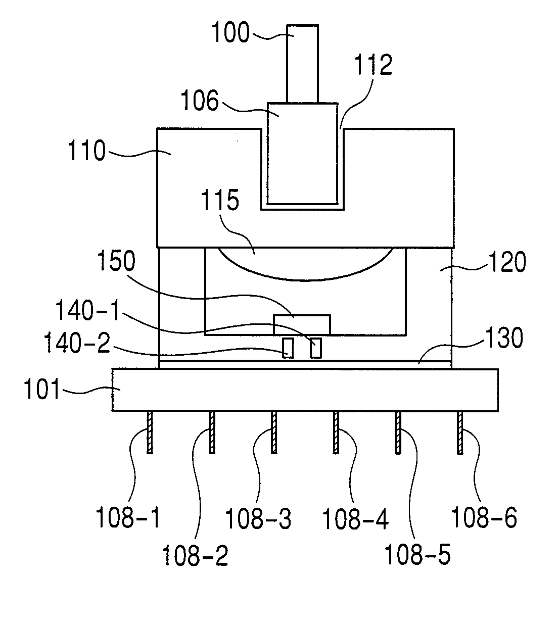
[0046]One end of each of the pins 108 is connected electrically to an external device to transmit electrical signals into the stem 101. The other end of each of the pins 108 is connected electrically to one of the through-via holes 140 through the electric wiring 130. In this first embodiment, the flip-chip bonding method is used to connect the optical element 150 to an electrode; both are connected electrically to each other through a through-via hole 140. This flip-chip bonding method can reduce the optical module in size, as well as enables band-widening when the inductance is lowered at electric connection points respectively. In this case, a bonding wire can also be used for the connection between the through-via hole 140 and the optical element 150.

[0047]If this optical element is a laser element, the light signal output from the optical element 150 according to an electric signal is condensed by the lens 115 and guided to the optical fiber 100 through the sealing substrate 11...

second embodiment

[0054]FIG. 3 is a cross sectional view of an optical module in the present invention. This structure is that of the optical modules referred to as receptacle ones. In case of this receptacle type optical module, optical fibers having connectors respectively can be attached to or removed from the optical module. The optical module shown in FIG. 3 is provided with a part 300 referred to as a receptacle, which is fit in the fiber fitting recessed part 112 of the sealing substrate 110 shown in FIG. 2. FIG. 25 is a cross sectional view of the structure of the receptacle. The receptacle consists of a holder part 310, a sleeve 320, and an optical connector 330. The holder part 310 is made of metal or the like. The sleeve 320 holds the optical connector 330. The optical connector 330 consists of a fiber stub and a glass block. The sleeve 320 enables the ferrule 106 and the optical connector 330 to be aligned to each other precisely. With this sleeve 320, optical signals can be exchanged bet...

third embodiment

[0055]FIG. 4 is a cross sectional view of an optical module in the present invention. In this configuration of the optical module, an external lens is used as the lens 115. The groove of the optical element mounting substrate 120 is formed by etching so as to be tapered forward. This means that the spacer is formed outside the groove. This spacer can also be formed as a separate part. In this case, because the spacer might be displaced on the optical element mounting substrate, the spacer should preferably be formed as part of the optical element mounting substrate by etching, for example. The lens 115 is disposed in this groove. The inside wall of the spacer (groove) should preferably be tapered forward so as to make it easier to position the light receiving part represented by this lens 115. The lens 115 should preferably be a spherical ball lens to reduce the manufacturing cost. Because the lens 115 is spherical and the spacer is tapered forward, the lens 115 can be fit easily in...


PUM


Abstract

An optical module is formed by sticking the optical element mounting substrate and the sealing substrate together, then by sealing the stuck body. The optical mounting substrate includes an optical element on its top surface and it is used to guide electrical signals to its back side through a through-via hole provided in itself. The sealing substrate includes a lens at its back side and a recessed part used to hold an optical fiber at its front side.

Description

CLAIM OF PRIORITY[0001]The present application claims priority from Japanese patent application JP 2009-071139 filed on Mar. 24, 2009, the content of which is hereby incorporated by reference into this application.FIELD OF THE INVENTION[0002]The present invention relates to an optical module, particularly to an optical module to be employed for optical communications to transmit a light with use of an optical fiber respectively.BACKGROUND OF THE INVENTION[0003]In recent years, optical communication traffics have been rapidly expanding to exchange large capacity data in the field of information communications. So far, optical fiber networks have been developed in order to meet the requirements of such optical communications in comparatively long distances of more than a few kilometers for trunk, metro, and access systems. And in the near future, optical fibers will also come to be used for signal wirings even in extremely short distances between transmission apparatuses (from a few m...

Claims


Application Information

Patent Timeline
Patent Type & Authority Applications(United States)
IPC IPC(8): G02B6/36
CPCG02B6/29365G02B6/4201G02B6/423G02B6/4215G02B6/4224G02B6/4204
Inventor SUGAWARA, TOSHIKIHOSOMI, KAZUHIKOMATSUOKA, YASUNOBUBAN, TAKUMAADACHI, KOICHIROLEE, YOUNGKUNAOKI, MASAHIRO
Owner HITACHI LTD
Why Eureka
Try Eureka