Method for forming an absorber layer of a thin film solar cell

a thin film solar cell and absorber layer technology, applied in the direction of sustainable manufacturing/processing, final product manufacturing, inks, etc., can solve the problems of unsuitable mass production solar cells, unsuitable for large surface area devices, unsuitable for mbe process, etc., to achieve low cost, improve solar cell efficiency, and large surface area

Inactive Publication Date: 2010-09-30
HONDA MOTOR CO LTD
View PDF3 Cites 36 Cited by
  • Summary
  • Abstract
  • Description
  • Claims
  • Application Information

AI Technical Summary

Benefits of technology

[0006]In view of such problems of the prior art, a primary object of the present invention is to provide a method for forming an absorber layer that allows a solar cell having a large surface area to be fabricated at low cost and the efficiency of the solar cell to be improved by forming a favorable band gap gradient structure.
[0009]Thus, by forming the absorber layer with a plurality of thin absorber sub-layers each having a controlled band gap, a solar cell having a large surface area can be fabricated at low cost and the efficiency of the solar cell can be improved by forming a favorable band gap gradient structure. As these sub-layers can be applied simply by any known processes, including spin-coating, bar coating, dip coating, contact and non-contact printing methods, the method of the present invention is highly suited to be used for mass producing solar cells.
[0010]In implementing the present invention, it is important to rapidly bake each sub-layer so as to minimize thermal effect on the underlying sub-layer. Therefore, the dried sub-layer of the mixture is rapidly baked preferably by radiating infrared energy or laser energy thereon.
[0011]According to a preferred embodiment of the present invention, the mixtures are prepared by mixing a first mixture and a second mixture at different mixing ratios, the first mixture containing Cu, Se, In and optional Ga at a substantially smaller composition ratio as compared to In, and the second mixture containing Cu, Se, Ga and optional In at a substantially smaller composition ratio as compared to Ga. Thereby, the fabrication process can be simplified.
[0012]The liquid medium may comprise an organic solvent such as toluene. In particular, the mixtures may be prepared by mixing small particles preferably of a nanometer order of members selected from a group consisting of Ga, In, Ga compound and In compound in the liquid medium so that the conversion efficiency of the fabricated solar cells may be maximized.

Problems solved by technology

The chalcopyrite thin film solar cell can be manufactured by a variety of manufacturing processes from a wide range of materials, and is therefore susceptible of low cost manufacture and improvement in performance.
However, the MBE process is considered to be unsuitable for mass producing solar cells as it is required to be performed in a high vacuum environment, and is not only expensive and time consuming to perform but also unsuitable for processing large surface area devices.
There may be other vapor deposition processes and sputtering processes that may be considered as being suitable for mass production, but they do not allow a precise control of composition because of various reasons such as the limitations in the composition of the sputter targets.
Therefore, these processes are unsuitable for providing a desired band gap gradient structure.

Method used


Image

  • Method for forming an absorber layer of a thin film solar cell
  • Method for forming an absorber layer of a thin film solar cell
  • Method for forming an absorber layer of a thin film solar cell

Examples


Embodiment Construction

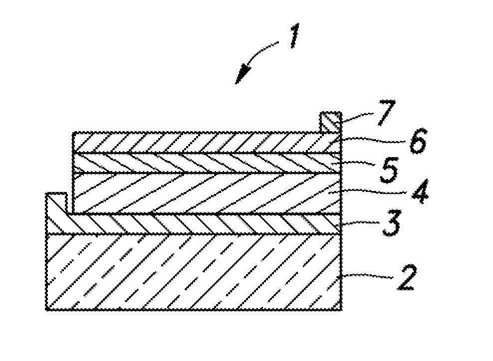
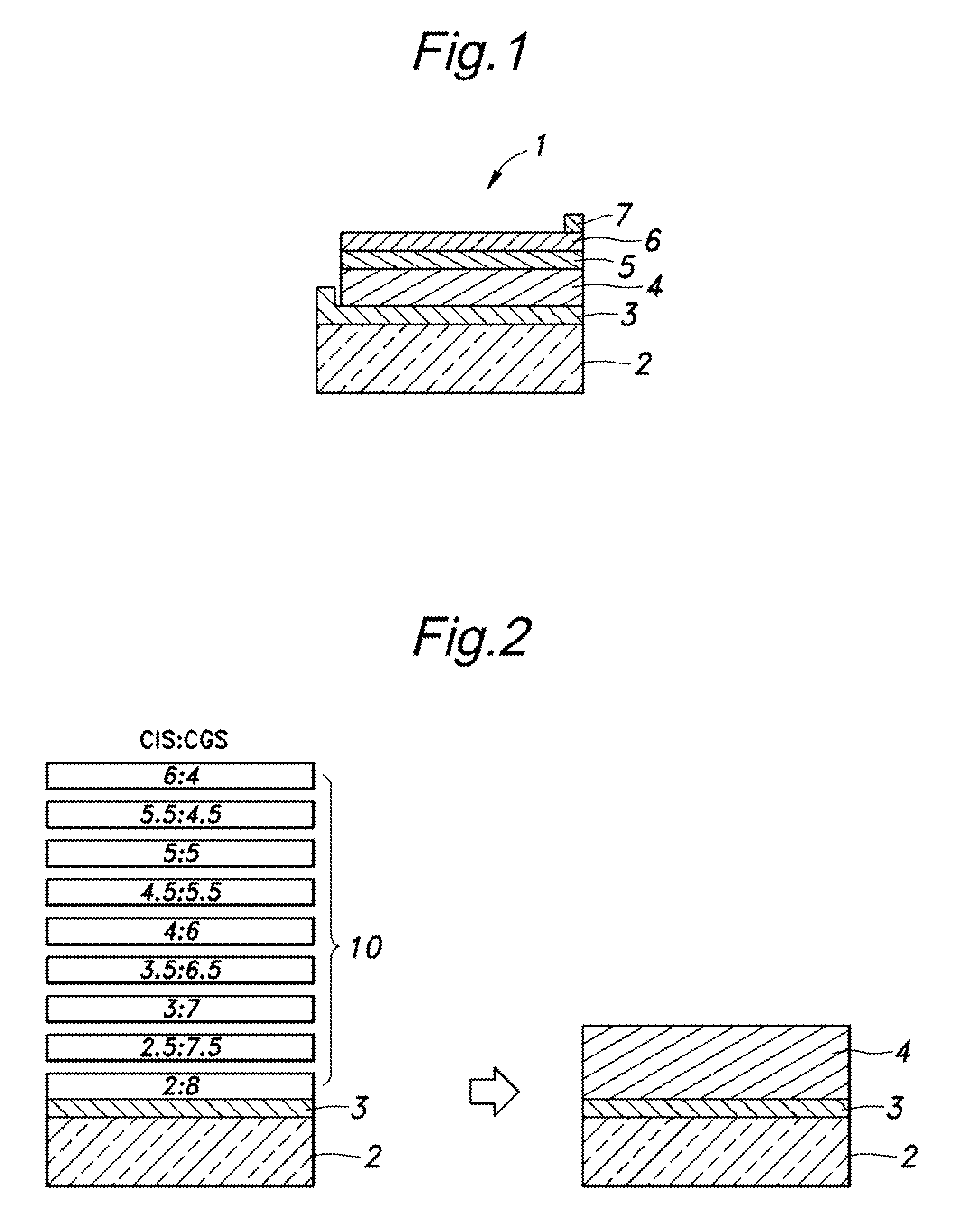
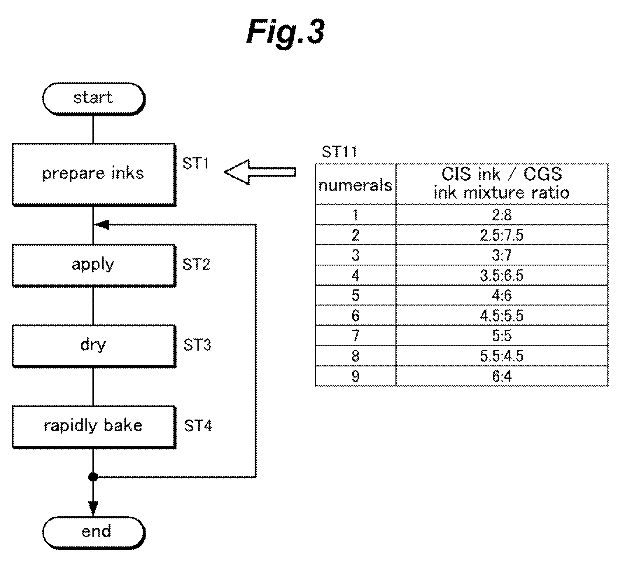
[0019]A preferred embodiment of the present invention is described in the following with reference to the appended drawings. FIG. 1 is a diagrammatic sectional view of a chalcopyrite solar cell incorporated with an absorber layer embodying the present invention. The solar cell 1 is provided with a laminated structure including a substrate 2, a back electrode layer 3 forming a positive pole of the solar cell 1, a CIGS absorber layer 4, a buffer layer 5 and a transparent electrode layer 6 stack one above another in that order. The solar cell 1 is additional provided with an electrode 7 electrically connected to the transparent electrode layer 6, and forming a negative pole of the solar cell 1.

[0020]The substrate 2 consists of sheet glass in the illustrated embodiment, but may also consist of other materials such as a metallic foil, a plastic sheet and so on which may be more light weight and / or flexible. The back electrode layer 3 consists of a Mo film in the illustrated embodiment, b...


PUM

PropertyMeasurementUnit
thicknessaaaaaaaaaa
thicknessaaaaaaaaaa
particle sizeaaaaaaaaaa

Abstract

In a method for forming a light absorber layer (4) of a thin film solar cell, the absorber layer is formed from a plurality of sub-layers each of which is formed by preparing a plurality of mixtures containing Cu, Se, In and Ga in a liquid medium, a composition ratio of In to Ga being progressively increased from one mixture to another, the mixtures optionally including a mixture containing no In or Ga; applying a layer of one of the mixtures onto a back electrode layer (3) formed on a substrate (2); drying the applied layer of the mixture; and rapidly baking the dried layer of the mixture. By forming the absorber layer with a plurality of thin absorber sub-layers each having a controlled band gap, a solar cell having a large surface area can be fabricated at low cost and the efficiency of the solar cell can be improved by forming a favorable band gap gradient structure. As these sub-layers can be applied simply by any known processes, the method of the present invention is highly suited to be used for mass producing solar cells.

Description

RELATED APPLICATIONS[0001]The present application claims foreign priority benefit under 35 U.S.C. §119 from earlier filed Japanese Patent Application No. 2009-071255 filed on Mar. 24, 2009, the disclosure of which is incorporated by reference herein in its entirety for all purposes.TECHNICAL FIELD[0002]The present invention relates to a method for forming a light absorber layer of a chalcopyrite thin film solar cell.BACKGROUND OF THE INVENTION[0003]The chalcopyrite thin film solar cell can be manufactured by a variety of manufacturing processes from a wide range of materials, and is therefore susceptible of low cost manufacture and improvement in performance. For this reason, solar cells of this type have been the subject of intensified research and development efforts by a number of research institutions and manufacturing corporations. In recent years, commercialization of chalcopyrite thin film solar cells are being accelerated because of the ease in fabricating large area devices...

Claims


Application Information

Patent Timeline
Patent Type & Authority Applications(United States)
IPC IPC(8): H01L31/18
CPCC09D11/101H01L21/02425H01L21/02485H01L21/0251H01L21/02568Y02E10/541H01L21/02628H01L31/0322H01L31/03928H01L31/065H01L31/0749H01L21/02601Y02P70/50
Inventor OKAMURA, DAISUKEKUBOTA, TADAHIRONOSAKI, KATUSTOSHI
Owner HONDA MOTOR CO LTD
Why Eureka
Try Eureka