System having a plurality of memory devices and data transfer method for the same

a technology of memory devices and data transfer methods, which is applied in the direction of digital storage, electric digital data processing, instruments, etc., can solve the problems of insufficient consideration of the dependability of communication communication faults may occur between the control unit provided, and the risk of memory contents errors such as memory errors, so as to achieve reliable high-speed data transfer and reduce consumption current

Active Publication Date: 2010-10-07
SEIKO EPSON CORP
View PDF25 Cites 53 Cited by
  • Summary
  • Abstract
  • Description
  • Claims
  • Application Information

AI Technical Summary

Benefits of technology

[0009]An object of the present invention is to achieve dependable high-speed data transfers in a system having a p

Problems solved by technology

However, in conventional techniques, insufficient consideration is given to the issue of dependability of communication between the control unit provided to the printer and the memory devices provided to the ink receptacles.
For example, there is a risk that, for reasons such as faulty contact between the electrical contact portions of the printer and an ink receptacle, communication faults may occur between the control unit provided to the printer and the memory device of the ink receptacle.
If operation of the print control unit is continued on with the communication fault unresolved, there is a risk of

Method used


Image

  • System having a plurality of memory devices and data transfer method for the same
  • System having a plurality of memory devices and data transfer method for the same
  • System having a plurality of memory devices and data transfer method for the same

Examples


embodiment 1

B. Embodiment 1

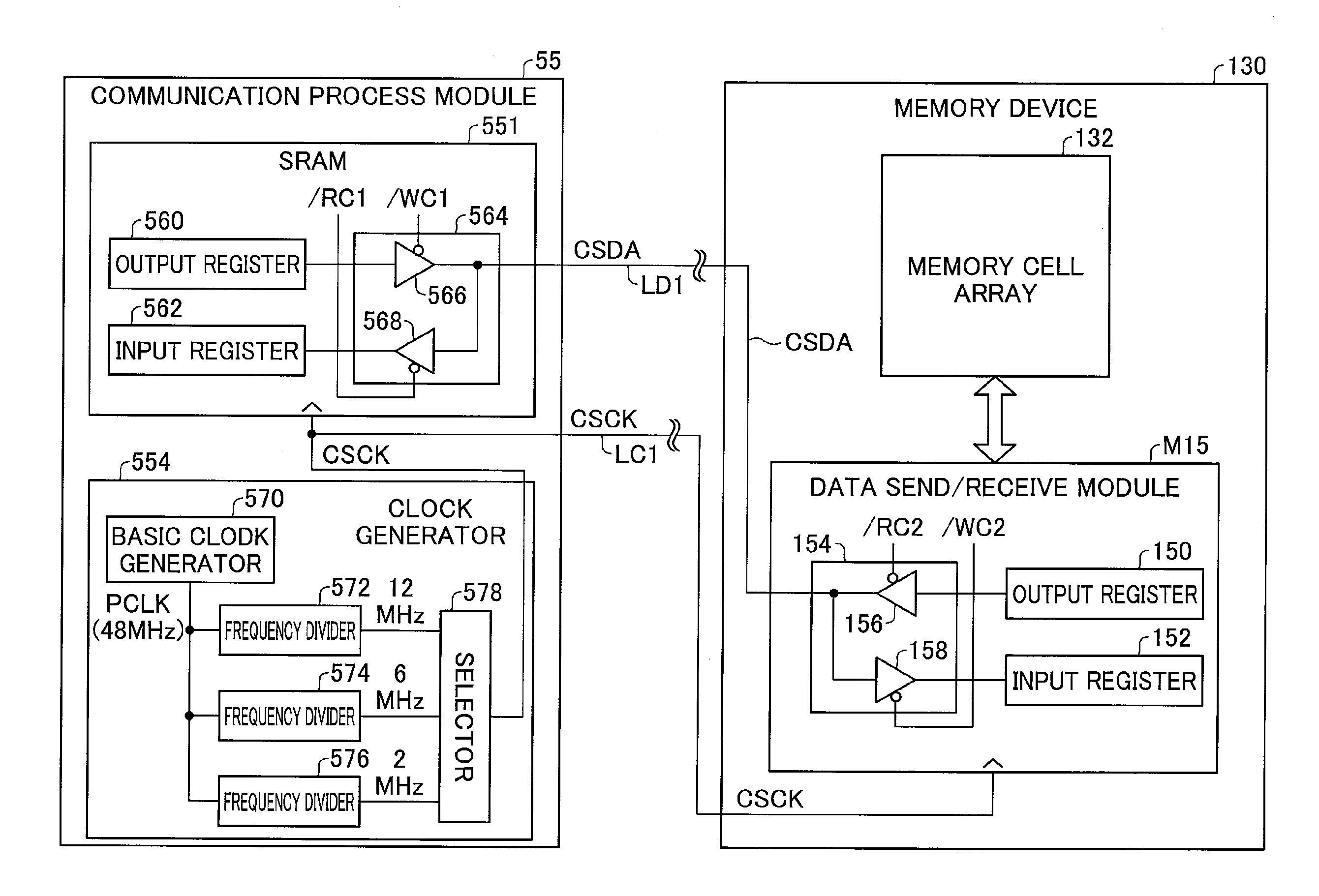
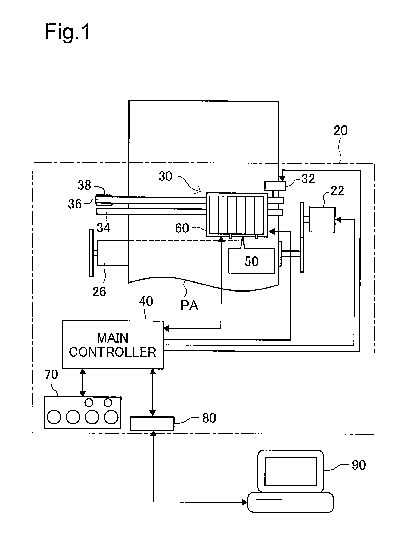
[0065]FIG. 6 is a block diagram depicting functional configuration of the main control circuit 40 and functional configuration of the sub-controller 50 and an ink cartridge 100 in Embodiment 1. The main controller 40 is provided with a control circuit 48, a drive signal generating circuit 42, and ROM, RAM, EEPROM or the like. Various programs for controlling the printer 20 are stored in the ROM. The control circuit 48 has a CPU (central processing unit), and performs control of the printer 20 as a whole in cooperation with the ROM, RAM, EEPROM or other memory. The control circuit 48 is provided as function blocks with a remaining ink level detection module M1, a memory access module M2, and a ink consumption estimation module M3. It should be noted that “modules” and “sections” are used as synonyms in the specification.

[0066]The remaining ink level detection module M1 controls the sub-controller 50 and the drive signal generating circuit 42, drives the sensor 110 of t...

embodiment 2

C. Embodiment 2

[0114]FIG. 12 is a block diagram depicting functional configuration of the main control circuit 40 and functional configuration of the sub-controller 50 and an ink cartridge 100 in Embodiment 2, and corresponds to FIG. 6 of Embodiment 1. The only difference from the circuit configuration depicted in FIG. 6 is that the memory control circuit 136 of the memory device 130 is additionally furnished with a copy data generation module M17, an inverted data generation module M18, and a data determination module M19; the configuration is otherwise the same as in FIG. 6. As will be discussed later, in Embodiment 2 inverted data and mirror data are sent in addition to the data proper (termed “original data”) as read data or write data. The copy data generation module M17 has the function of copying the original data to generate mirror data equal in size to the original data. The inverted data generation module M18 is adapted to invert the value of each bit of the original data ...

modified embodiment 1

[0224]In Embodiment 2 above, inverted data / Dn of the original data Dn is used as the related data for checking consistency with the original data Dn; however, other data having a prescribed logical relationship to the original data Dn may be used instead. As specific examples, related data such as the following may be used.

(1) A copy of the original data Dn

(2) Data resulting from addition of a prescribed value to the original data Dn

(3) Data resulting from subtraction of a prescribed value from the original data Dn

(4) Data resulting from multiplication of the original data Dn by a prescribed value

(5) Data resulting from a prescribed bit shift operation performed on the original data Dn

(6) Data resulting from a prescribed bit rotation operation performed on the original data Dn

[0225]Generally, it suffices for the original data Dn and the related data which is related to the original data Dn to have a prescribed logical relationship to one another, such that that the presence or lack...


PUM


Abstract

The control section performs a write operation, in synchronism with a clock signal, for transferring write data to one of the plurality of memory devices, utilizing: (i) an identification information transmission period during which the control section sends the identification information of a single memory device to all of the plurality of memory devices through the data line to select the single memory device; (ii) a write data transmission period during which the control section sends a single set of write data having a prescribed size to the selected single memory device; and (iii) a response period during which the selected single memory device responds to the control section with a response signal indicating presence or absence of communication error in relation to the received set of write data. Communications between the control section and the selected memory device during the write data transmission period and the response period are repeatedly performed for each transmission of one of plural sets of write data having the prescribed size. The control section sets a frequency of the clock signal during the response period to a lower value than that of the clock signal during the write data transmission period.

Description

CROSS-REFERENCE TO RELATED APPLICATIONS[0001]The present application claims the priority based on Japanese Patent Applications No. 2009-088591 filed on Apr. 1, 2009, and No. 2009-269529 filed on Nov. 27, 2009, the disclosures of which are hereby incorporated by reference in their entireties.BACKGROUND OF THE INVENTION[0002]1. Field of the Invention[0003]The present invention relates to a system furnished with a plurality of memory devices, and particularly to a data transfer technique for the same.[0004]2. Description of the Related Art[0005]An inkjet printer, which is one example of liquid ejecting apparatus, typically has one or more installed ink receptacles provided as detachable liquid receptacles. Some ink receptacles are furnished with memory devices. The memory device stores information of various kinds, for example, the remaining ink level or the color of the ink in the ink receptacle (see JP 2002-370383 A, JP 2004-299405 A). A control unit provided to the printer communica...

Claims


Application Information

Patent Timeline
IPC IPC(8): G11C7/10G11C8/18
CPCG06F13/4291
Inventor ASAUCHI, NOBORU
Owner SEIKO EPSON CORP
Why Eureka
Try Eureka