Bonding of substrates including metal-dielectric patterns with metal raised above dielectric

a technology of dielectric pattern and substrate, applied in the direction of manufacturing tools, non-electric welding apparatus, transportation and packaging, etc., can solve the problems of preventing a reliable bond, non-uniform metal surface, and many challenges of thermal compression bonding, and achieve good electrical and thermal connection, strong bonding medium, and enhanced functionality

Active Publication Date: 2010-10-07
GLOBALFOUNDRIES US INC
View PDF8 Cites 30 Cited by
  • Summary
  • Abstract
  • Description
  • Claims
  • Application Information

AI Technical Summary

Benefits of technology

[0008]Bonding of substrates including metal-dielectric patterns on a surface with the metal raised above the dielectric is disclosed. One method includes providing a first substrate having a metal-dielectric pattern on a surface thereof; providing a second substrate having a metal-dielectric pattern on a surface thereof; performing a process resulting in the metal being raised above the dielectric in at least one of the substrates; cleaning the metal; and bonding the first substrate to the second substrate. A related structure is also disclosed. The bonding of raised metal provides a strong bonding medium, and good electrical and thermal connections enabling creation of three dimensional integrated structures with enhanced functionality.

Problems solved by technology

Unfortunately, thermal compression bonding presents many challenges in order to achieve a good quality bond.
One challenge is optimizing process parameters.
Another challenge is addressing patterned metal-dielectric mating surfaces that typically include topography, which prevents a reliable bond.
CMP, however, leaves the metal surface non-uniform, e.g., the metal is typically concave and non-planar relative to the dielectric.
As a result, the topographical differences between bonding metallic surfaces presents a challenge.
Unfortunately, the non-uniformity and the difference in the distances between bonding metallic surfaces does not always allow for adequate bonding via reflow, resulting in low yields.

Method used


Image

  • Bonding of substrates including metal-dielectric patterns with metal raised above dielectric
  • Bonding of substrates including metal-dielectric patterns with metal raised above dielectric
  • Bonding of substrates including metal-dielectric patterns with metal raised above dielectric

Examples


Embodiment Construction

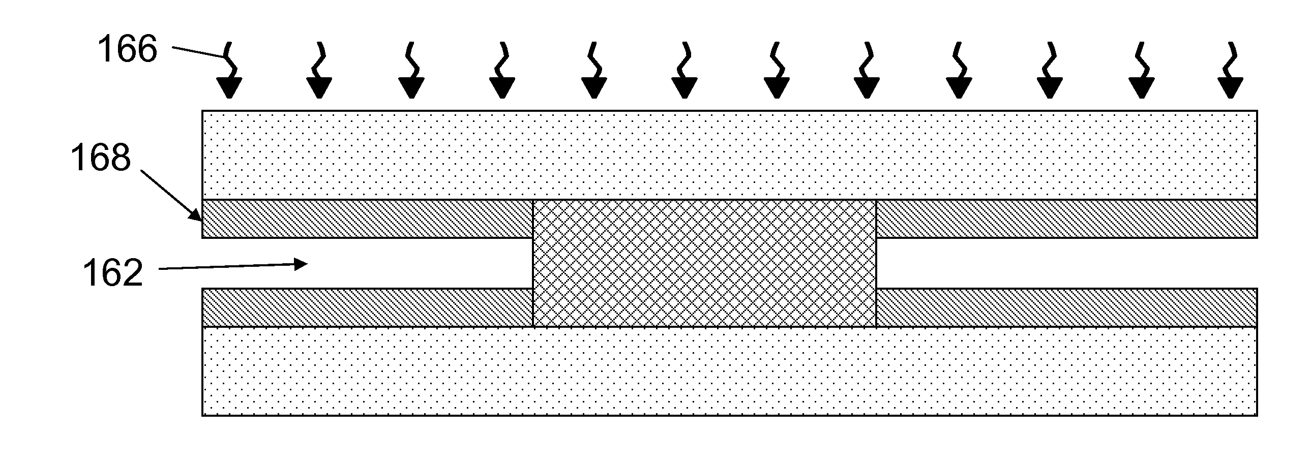
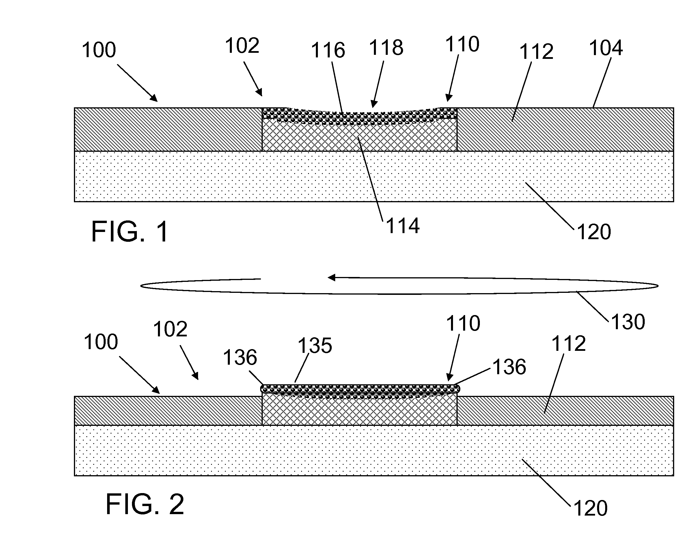
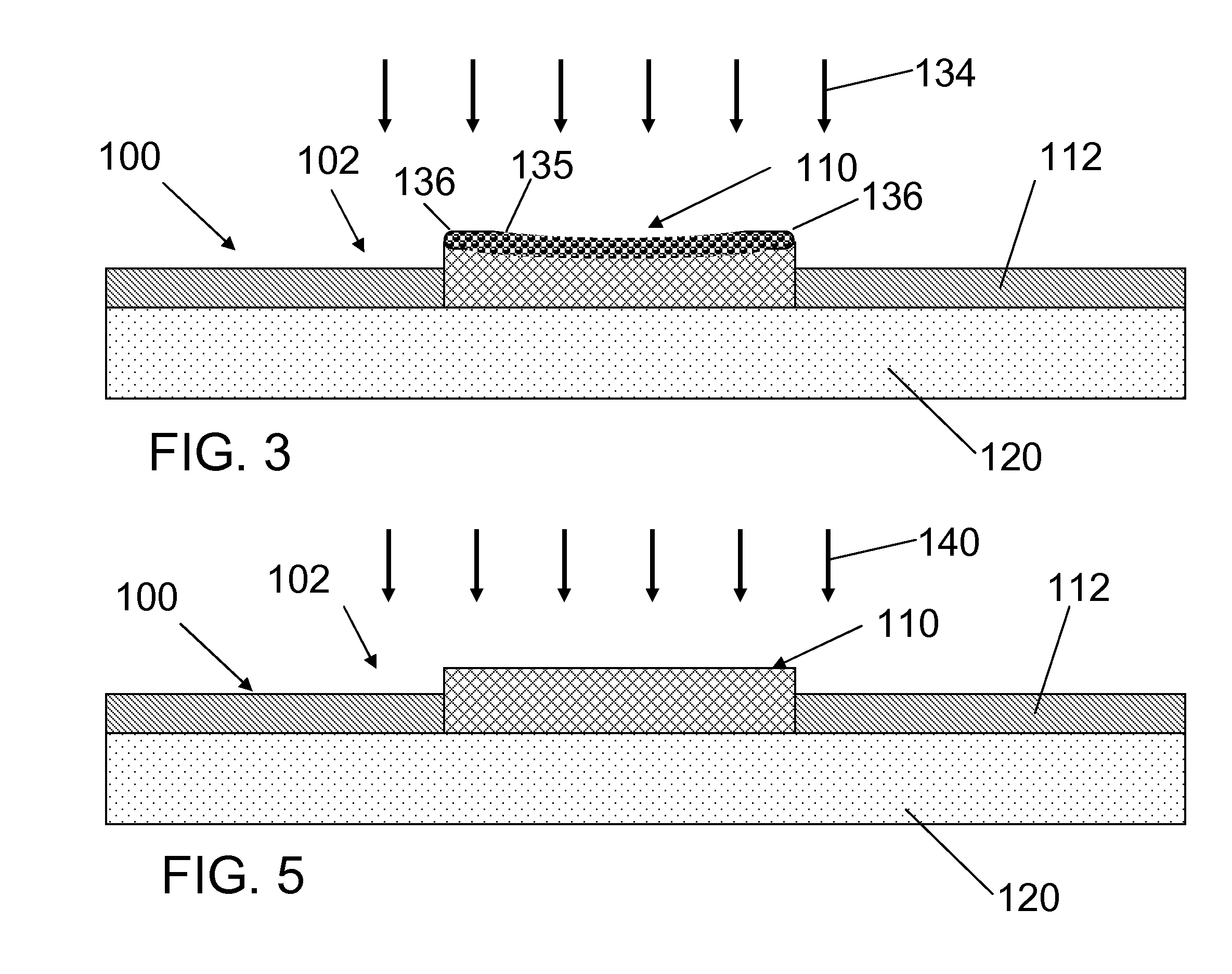
[0029]Turning to the drawings, FIGS. 1-9 show one embodiment of a method of bonding according to the invention. FIG. 1 shows a substrate 100 having a metal-dielectric pattern 102 on a surface 104 thereof. As will be described herein, two substrates 100 having metal-dielectric patterns 102 will ultimately be provided and bonded together. Metal-dielectric pattern 102 includes a metal 110 such as a wire or contact positioned within a dielectric 112. It is understood that the layout of metal 110 within the different substrates may vary according to the functioning of the integrated circuit (IC) formed thereby. Metal 110 may include any now known or later developed metallic material 114, e.g., copper, tungsten, aluminum, etc., or combination thereof. In addition, metal 110 may include an oxide layer 116 thereover, e.g., where it has been exposed to the environment. Dielectric 112 may include any now known or later developed insulator material usable in bonded substrates 100, e.g., silico...


PUM

PropertyMeasurementUnit
metal-dielectricaaaaaaaaaa
dielectricaaaaaaaaaa
temperatureaaaaaaaaaa

Abstract

Bonding of substrates including metal-dielectric patterns on a surface with the metal raised above the dielectric is disclosed. One method includes providing a first substrate having a metal-dielectric pattern on a surface thereof; providing a second substrate having a metal-dielectric pattern on a surface thereof; performing a process resulting in the metal being raised above the dielectric; cleaning the metal; and bonding the first substrate to the second substrate. A related structure is also disclosed. The bonding of raised metal provides a strong bonding medium, and good electrical and thermal connections enabling creation of three dimensional integrated structures with enhanced functionality.

Description

GOVERNMENT INTEREST[0001]This invention was made with government support under contract numbers: N66001-00-C-8003 and N66001-04-C-8032 of the Defense Advanced Research Projects Agency (DARPA). The government has certain rights to this invention.BACKGROUND OF THE INVENTION[0002]1. Technical Field[0003]The invention generally relates to the integrated circuit fabrication and, more specifically, to bonding of substrates having metal-dielectric patterns.[0004]2. Background Art[0005]In the integrated circuit fabrication industry, substrate bonding is used to join various parts of an integrated circuit (IC) together. Thermal-compression bonding is one type of bonding that is advantageous because it allows the use of metals at the bonding interface rather than just dielectrics. The metallic surface serves as a good bonding medium, and also provides additional functionality such as electrical signal propagation and thermal spreading. Unfortunately, thermal compression bonding presents many ...

Claims


Application Information

Patent Timeline
Patent Type & Authority Applications(United States)
IPC IPC(8): B32B3/00B23K31/02
CPCB23K20/023Y10T428/24521B23K20/24B23K2201/42H01L24/12H01L24/05H01L2224/08147H01L24/03H01L24/08H01L24/80H01L2224/0381H01L2224/03845H01L2224/05571H01L2224/80895H01L2224/80896H01L2224/80203H01L2224/80345H01L2224/05572H01L2224/08148H01L2224/80948B23K20/233Y10T428/24479Y10T428/24545Y10T428/24612H01L2924/1461H01L2924/00012H01L2924/0001H01L2224/80986H01L2224/0401H01L2924/14Y10T428/31678B23K2101/42H01L2224/8034H01L2224/08145H01L2924/00
Inventor CHEN, KUAN-NENGFURMAN, BRUCE K.PURUSHOTHAMAN, SAMPATHRATH, DAVID L.TOPOL, ANNA W.TSANG, CORNELIA K.
Owner GLOBALFOUNDRIES US INC
Why Eureka
Try Eureka