Method of manufacturing thin film device and thin film device manufactured using the same

a technology of thin film and manufacturing method, which is applied in the direction of semiconductor devices, electrical devices, chemistry apparatus and processes, etc., can solve the problems of difficult to ensure the high performance of the functional unit formed, and achieve the effect of simplifying the entire process and excellent properties

Inactive Publication Date: 2010-10-07
SAMSUNG ELECTRO MECHANICS CO LTD
View PDF6 Cites 21 Cited by
  • Summary
  • Abstract
  • Description
  • Claims
  • Application Information

AI Technical Summary

Benefits of technology

[0010]An aspect of the present invention provides a method of a thin film device for sim

Problems solved by technology

However, since it is difficult to ensure the high performance of the functional unit formed of the organic thin film, it is necessary to form a functional unit of the flexible device by the use of an inorganic material.
In this case, since it is difficult to apply a high-temperature deposi

Method used


Image

  • Method of manufacturing thin film device and thin film device manufactured using the same
  • Method of manufacturing thin film device and thin film device manufactured using the same
  • Method of manufacturing thin film device and thin film device manufactured using the same

Examples


Embodiment Construction

[0028]Exemplary embodiments of the present invention will now be described in detail with reference to the accompanying drawings.

[0029]FIGS. 1A through 1F are schematic cross-sectional views illustrating a series of processes in a method of manufacturing a thin film device according to an exemplary embodiment of the present invention.

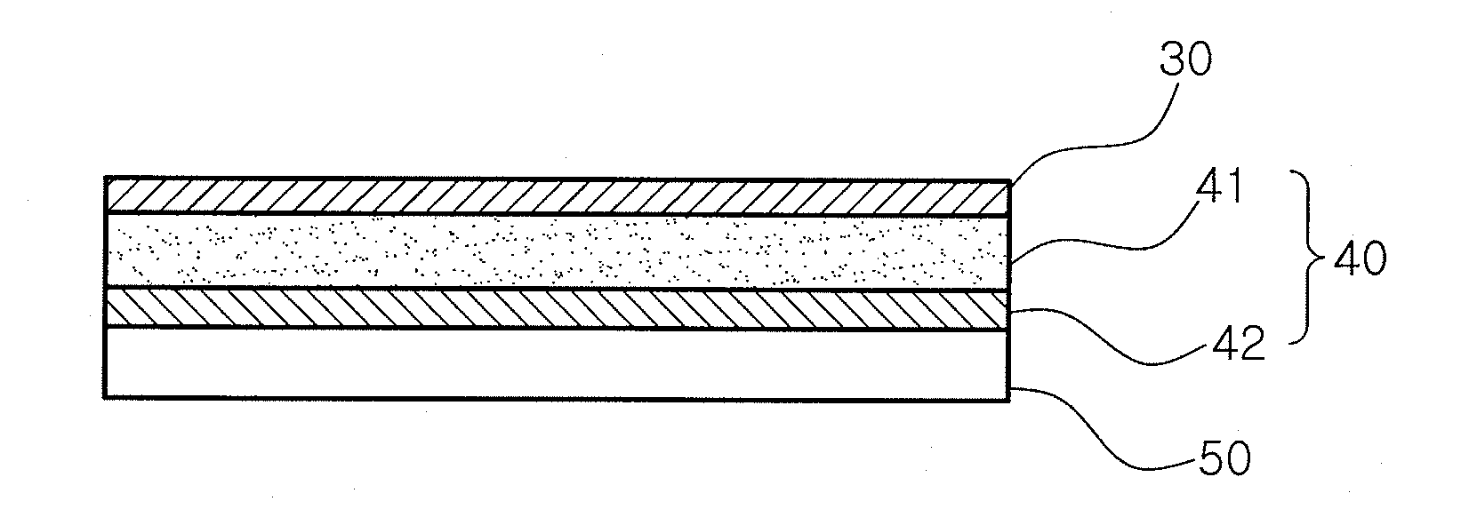
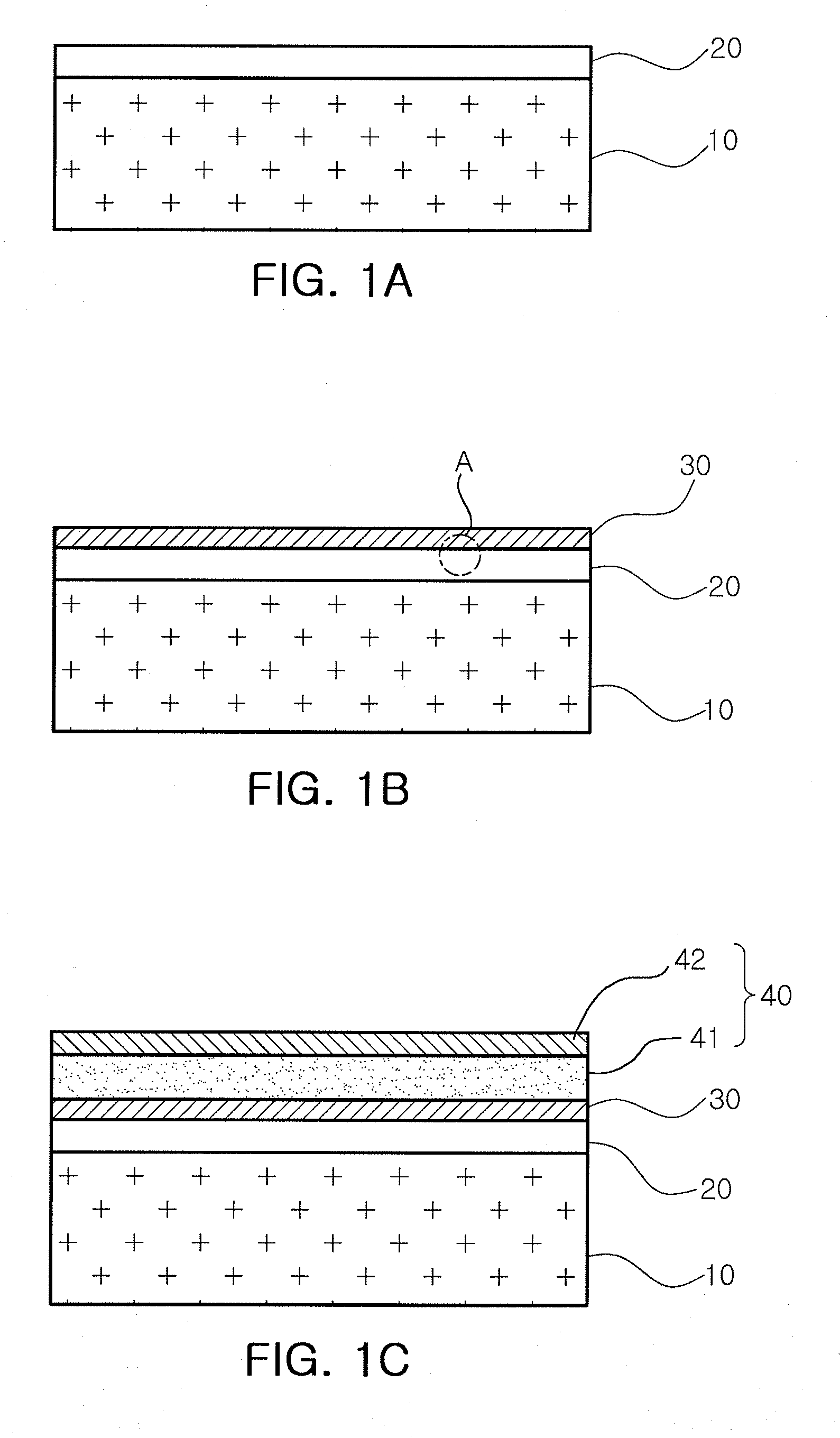
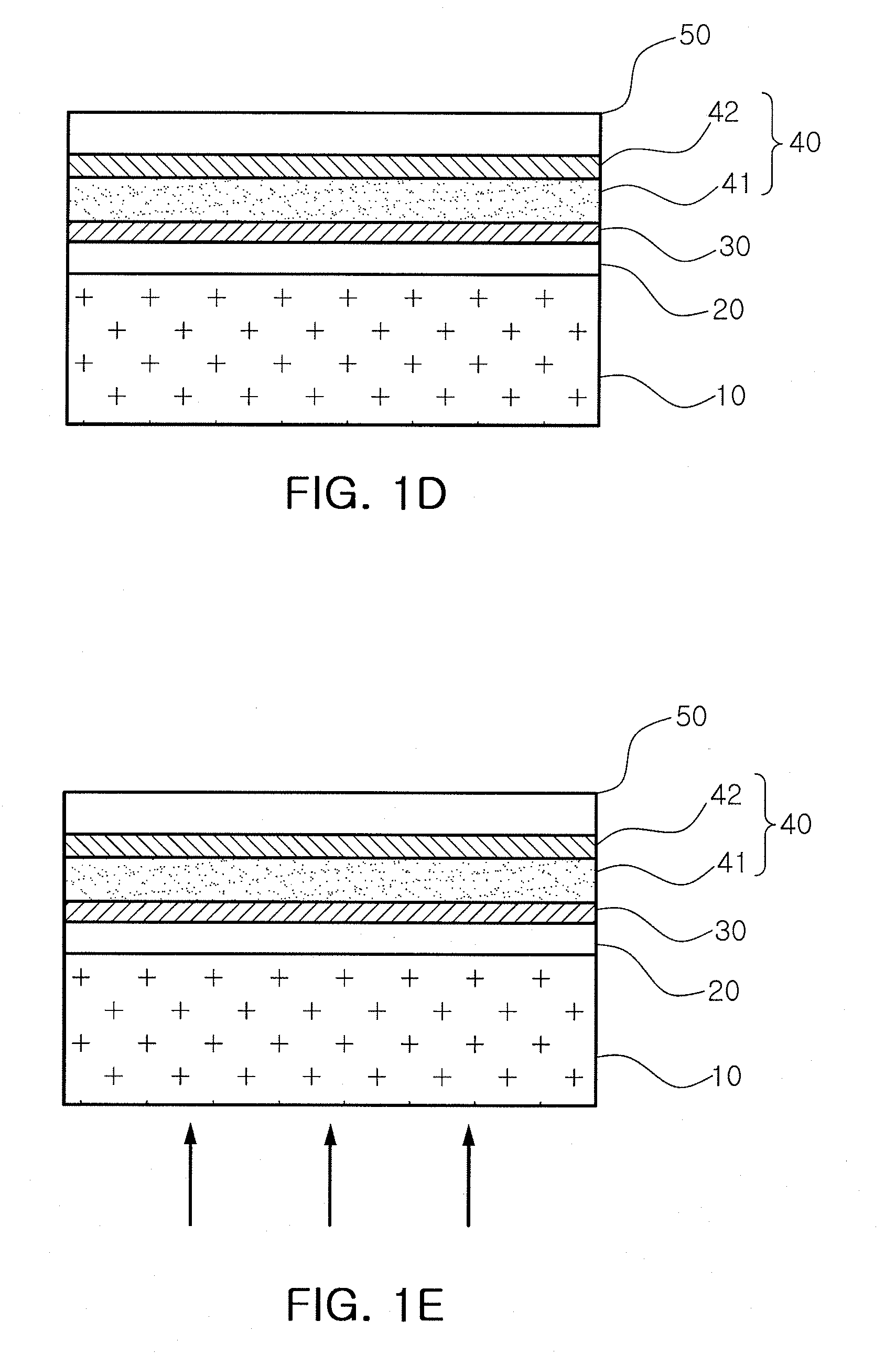
[0030]First of all, as illustrated in FIG. 1A, a preliminary substrate 10 is prepared, and then a sacrificial layer 20 is deposited on the preliminary substrate 10 by the use of a first oxide having a perovskite structure (ABO3). The preliminary substrate 10 may be transmitted by the laser and have a greater band gap than the energy corresponding to a wavelength of the laser.

[0031]The preliminary substrate 10 may be suitable for forming a thin film serving as a particular functional device. For example, when a desired thin film requires high-temperature deposition conditions, the preliminary substrate may be formed of a material having thermal resistanc...


PUM

PropertyMeasurementUnit
Temperatureaaaaaaaaaa
Dielectric polarization enthalpyaaaaaaaaaa
Flexibilityaaaaaaaaaa

Abstract

There is provided a method of manufacturing a thin film device and a thin film device manufactured using the same. The method includes forming a sacrificial layer using a first oxide having a perovskite structure on a preliminary substrate; forming an electrode layer using a second oxide having a perovskite structure on the sacrificial layer; forming a thin film laminate on the electrode layer; bonding a permanent substrate onto the thin film laminate; decomposing the sacrificial layer by irradiating a laser onto the preliminary substrate; and separating the preliminary substrate from the electrode layer. During a laser lift-off process, degradation of properties caused by oxygen diffusion can be prevented. Since the electrode layer has thermal conductivity lower than an existing metal electrode, heat emission can be considerably reduced and the sacrificial layer can be easily decomposed by heat accumulation. Therefore, a thin film device having excellent properties can be manufactured.

Description

CROSS-REFERENCE TO RELATED APPLICATIONS[0001]This application claims the priority of Korean Patent Application No. 2009-0029520 filed on Apr. 6, 2009, in the Korean Intellectual Property Office, the disclosure of which is incorporated herein by reference.BACKGROUND OF THE INVENTION[0002]1. Field of the Invention[0003]The present invention relates to a method of manufacturing a thin film device and a thin film device manufactured using the same, and more particularly, to a method of manufacturing a thin film device using a simplified laser lift-off process and a thin film device having excellent properties.[0004]2. Description of the Related Art[0005]In general, a thin film transfer technique has been widely used in electronic devices such as a thin film transistor (TFT) and optical devices such as an organic EL device.[0006]The thin film transfer technique generally refers to a technique that forms a thin film on a preliminary substrate and then transfers the thin film onto a perman...

Claims


Application Information

Patent Timeline
IPC IPC(8): B32B9/00H01L21/28
CPCH01L29/7869H01L21/268H01L27/1266
Inventor KIM, BOUM SEOCKOH, YONGSOOKIM, SANG JINLEE, HWAN-SOO
Owner SAMSUNG ELECTRO MECHANICS CO LTD
Why Eureka
Try Eureka