Wafer processing method

Active Publication Date: 2010-10-07
DISCO CORP
View PDF2 Cites 13 Cited by
  • Summary
  • Abstract
  • Description
  • Claims
  • Application Information

AI Technical Summary

Benefits of technology

[0006]The metal film is coated on the rear surface of the wafer formed with the ringlike reinforcing portion. Thereafter, it is difficult, however, to make the rear side of the device area flush with the rear side of the outer circumferential redundant area by grinding only the rear surface of the ringlike reinforc

Problems solved by technology

Thereafter, it is difficult, however, to make the rear side of the device area flush with the rear side of the outer circumferential redundant area by grinding only the rear surface of the ringlike reinforcing portion without any damage to the metal film on th

Method used


Image

  • Wafer processing method
  • Wafer processing method
  • Wafer processing method

Examples


Embodiment Construction

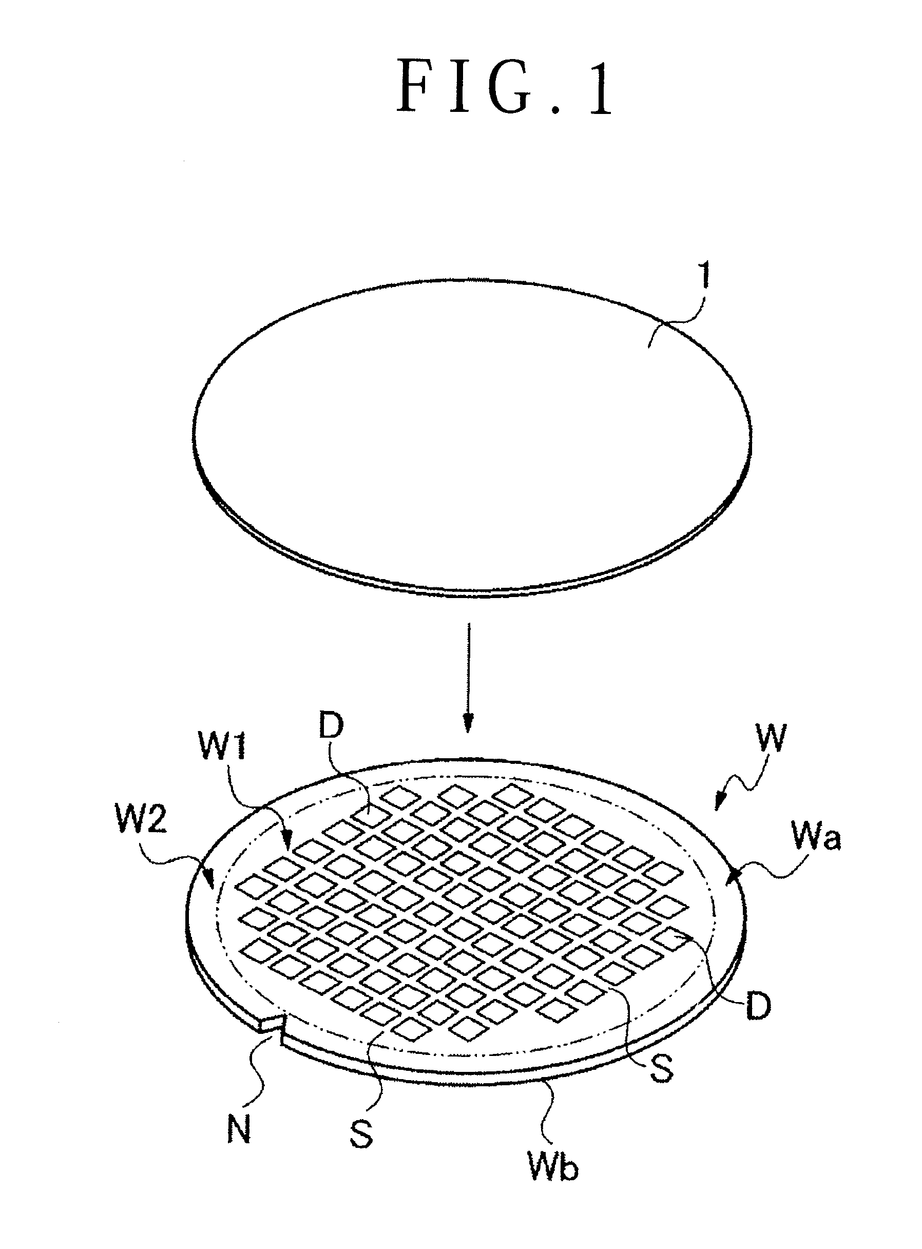
[0027]Referring to FIG. 1, a device area W1 formed with a plurality of devices D and an outer circumferential redundant area W2 surrounding the device area W1 and formed with no devices are formed on a front surface Wa of a wafer W. The device area W1 is sectioned by predetermined dividing lines S extending longitudinally and horizontally and is formed with the devices D. The wafer W shown as an example is formed on an outer circumferential portion with a notch N which is a mark for crystal orientation identification.

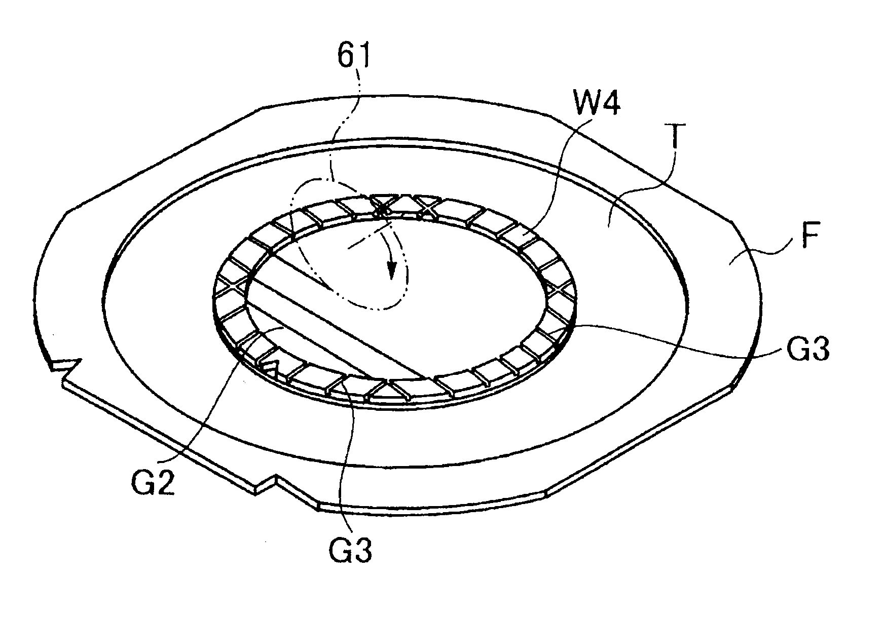
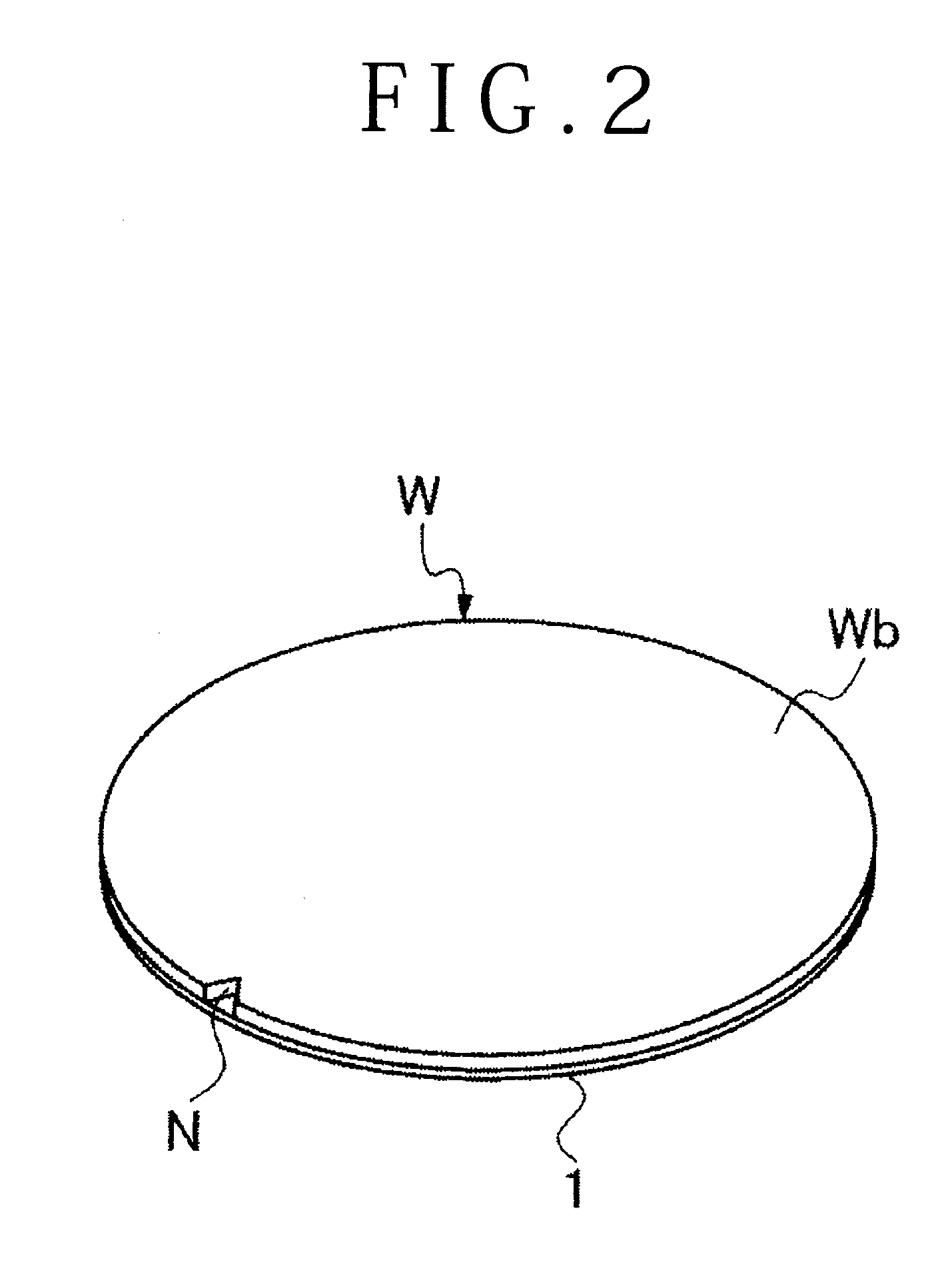
[0028]A protection tape 1 is stuck to the front surface Wa of the wafer W1, and the wafer W1 is turned back to expose a rear surface Wb as shown in FIG. 2. The rear surface Wb is ground using e.g. a grinding device 2 shown in FIG. 3. The grinding device 2 includes a chuck table 20 holding the wafer and being rotatable therewith and a grinding means 21 for grinding the wafer. The grinding means 21 includes a spindle 22 capable of being rotated and moved up and down, a gr...


PUM


Abstract

A wafer processing method of dividing a wafer into individual devices, the wafer having on a front surface a device area and an external circumferential redundant area surrounding the device area, the method including: a wafer grinding step in which, in the state where the wafer is held on the side of a protection tape stuck to the front surface of the wafer, a rear side of the device area in a rear surface of the wafer is ground to form a recessed portion to form a ringlike reinforcing portion on an outer circumferential side of the recessed portion; a metal film coating step for coating, with a metal film, a rear surface of the wafer stuck with the protection tape on the front surface; and a wafer dividing step for cutting the predetermined dividing lines from a rear surface side of the wafer stuck with the protection tape on the front surface, thereby dividing the wafer into the individual devices.

Description

BACKGROUND OF THE INVENTION[0001]1. Field of the Invention[0002]The present invention relates to a wafer processing method of grinding a rear surface of a wafer and dividing the wafer into individual devices.[0003]2. Description of the Related Art[0004]A wafer formed with a plurality of devices such as ICs is ground from the rear surface to have a given thickness and then divided by a dicing device or the like into individual devices, which are used in various electronic devices. In recent years, to make it possible to reduce the weight and size of electronic devices, a wafer has been formed by grinding to be as extremely thin as 100 to 20 μm. However, the wafer is formed thin to become soft, which poses problems for subsequent conveyance and of making it difficult to cover a ground surface with a metal film such as gold, silver, titanium or the like with a thickness of several tens nm for electrically testing devices.[0005]To eliminate such problems, the following wafer processing ...

Claims


Application Information

Patent Timeline
IPC IPC(8): H01L21/78H01L21/301H01L21/304
CPCH01L21/78H01L21/3043
Inventor PRIEWASSER, KARL
Owner DISCO CORP
Why Eureka
Try Eureka