Circuit for changing frequency of a signal and frequency change method thereof

Active Publication Date: 2010-10-21
SK HYNIX INC
View PDF9 Cites 12 Cited by
  • Summary
  • Abstract
  • Description
  • Claims
  • Application Information

AI Technical Summary

Benefits of technology

[0015]A signal frequency change circuit capable of minimizing a duty cycle error and r

Problems solved by technology

A semiconductor test device does not provide a suitable clock signal having a high frequency for testing the semiconductor integrated circuit.
Even though a structure of the signal frequency change circuit 1 according to the prior art is simple, problems can arise in that a duty cycle of the output signal ‘OUT’ significantly fluctuates according to the delay device ‘DLY’,

Method used


Image

  • Circuit for changing frequency of a signal and frequency change method thereof
  • Circuit for changing frequency of a signal and frequency change method thereof
  • Circuit for changing frequency of a signal and frequency change method thereof

Examples


Embodiment Construction

[0028]Hereinafter, preferred embodiments will be described in detail with reference to the accompanying drawings.

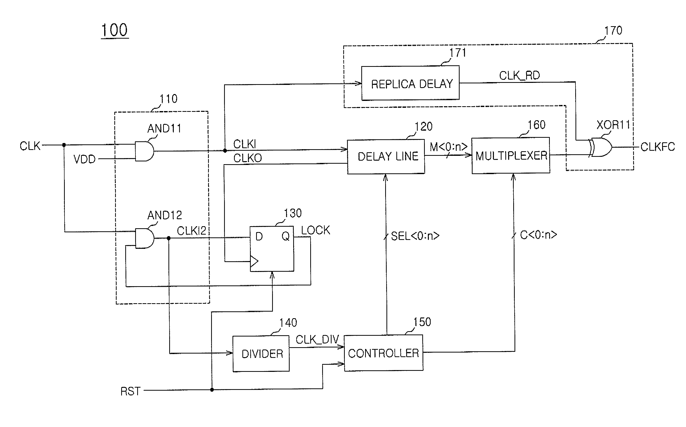
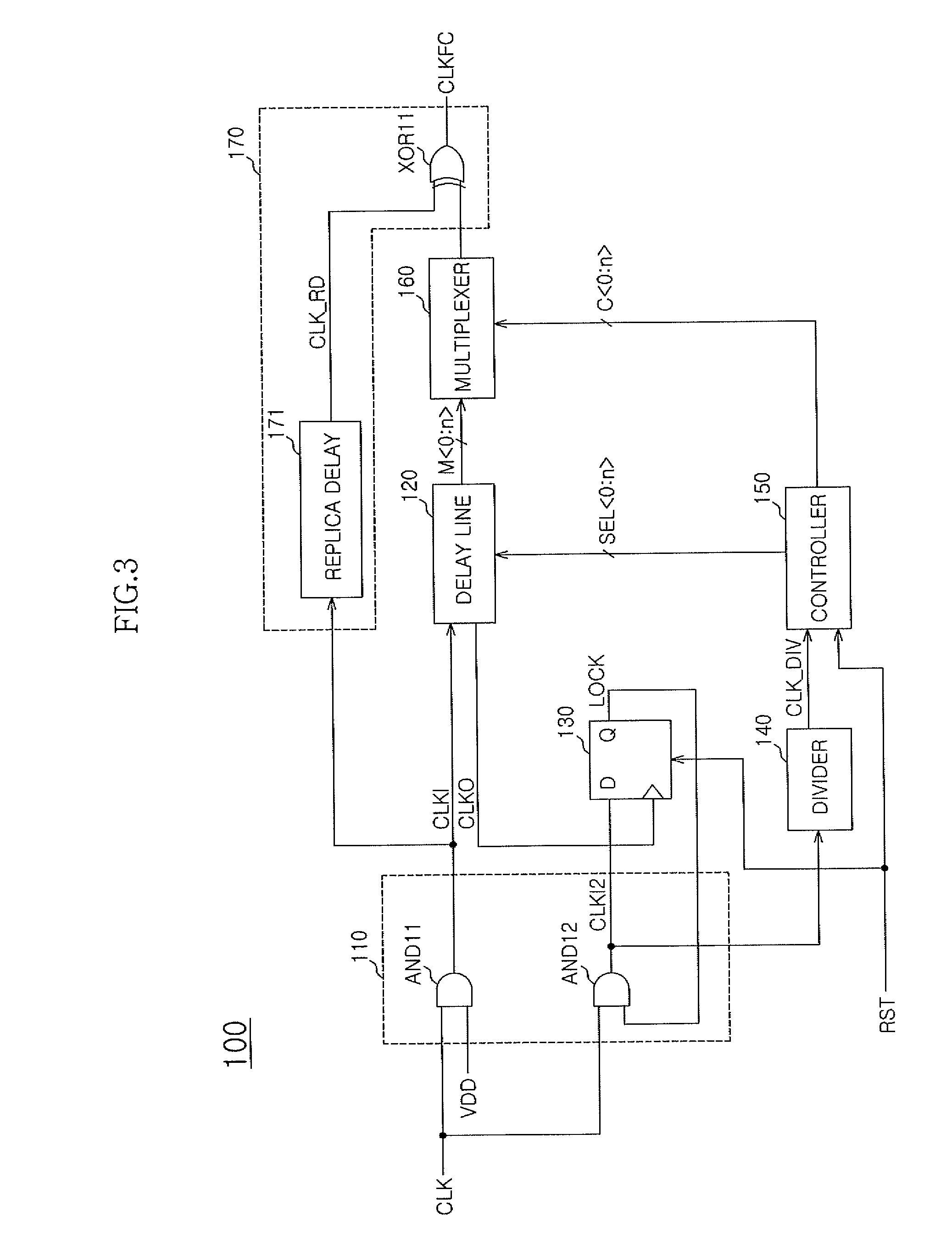
[0029]FIG. 3 is a block diagram of a signal frequency change circuit 100 according to the embodiment.

[0030]As shown in FIG. 3, the signal frequency change circuit 100 according to the embodiment includes an input unit 110, a delay line 120, a detector 130, a divider 140, a controller 150, a multiplexer 160, and an output unit 170.

[0031]The input unit 110 includes a first AND gate ‘AND11’ and a second AND gate ‘AND12’.

[0032]Since a power supply voltage ‘VDD’ is applied to a first input terminal, the first AND gate ‘AND11’ is provided with a clock signal ‘CLK’ input through a second input terminal to the delay line 120 as first input signal ‘CLKI’.

[0033]The second AND gate ‘AND12’ can transfer or interrupt the clock signal ‘CLK’ to the detector 130 in response to a phase locked completion signal ‘LOCK’. In other words, the second AND gate ‘AND12’ transfers a second input si...


PUM


Abstract

A signal frequency change circuit is presented. The signal frequency change circuit includes a delay line, a detector, a controller, a multiplexer, and an output unit. The delay line delays a clock signal by a first delay time corresponding to a delay control signal to generate a delay signal and delays the clock signal by a second delay time shorter than a first delay time to generate a pre-frequency change clock signal. The detector generates a phase locked completion signal. The controller sequentially shifts the delay control signal and a multiplexing control signal. The multiplexer selects and outputs one of the pre-frequency change clock signals. The output unit generates a frequency change clock signal.

Description

CROSS-REFERENCES TO RELATED PATENT APPLICATION[0001]The present application claims priority under 35 U.S.C 119(a) to Korean Application No. 10-2009-0032898, filed on Apr. 15, 2009, in the Korean Intellectual Property Office, which is incorporated herein by reference in its entirety as set forth in full.BACKGROUND[0002]1. Technical Field[0003]The present invention described herein relates to a semiconductor integrated circuit, and more particularly, to a circuit for changing a frequency of a signal and a frequency change method thereof.[0004]2. Related Art[0005]A semiconductor integrated circuit needs a clock signal having a frequency higher than a frequency of a clock signal provided from an external controller in order to test the operation thereof.[0006]A semiconductor test device does not provide a suitable clock signal having a high frequency for testing the semiconductor integrated circuit.[0007]Therefore, a signal frequency change circuit, which changes a frequency of a clock ...

Claims


Application Information

Patent Timeline
IPC IPC(8): H03B19/00
CPCG06F7/68H03K5/00006H03K5/133H03K2005/00058H03K5/135G01R31/3163G01R31/3181G01R31/3183
Inventor JEONG, CHUN SEOK
Owner SK HYNIX INC
Why Eureka
Try Eureka