
Resistance change memory device and operation method of the same

Active Publication Date: 2010-10-21
SONY SEMICON SOLUTIONS CORP
View PDF5 Cites 43 Cited by
  • Summary
  • Abstract
  • Description
  • Claims
  • Application Information

AI Technical Summary

Benefits of technology

[0012]It is desirable to provide a resistance change memory device which can be readily reduced in voltage when voltages of opposite polarity are applied to the storage element during data write and erase operations.
[0020]The above configuration allows for a voltage to be applied to the well during the second operation. Therefore, there is no need to apply a voltage to the storage element via the access transistor at least during the second operation. As a result, the voltage applied, for example, between the well and second wiring is applied almost as-is across the storage element, thus eliminating wasteful voltage drop. Therefore, it is only necessary to apply a voltage, equivalent to that required to change the data storage status of the storage element, for example, between the well and second wiring.
[0027]The present invention allows for a voltage to be applied without the source follower action of the access transistor, thus providing a resistance change memory device and operation method of the same which can be reduced in voltage.

Problems solved by technology

In order to operate the above 1T1R memory cell, therefore, the word line must be at a higher voltage than the voltage applied to the resistance change element, thus hindering the reduction in operating voltage.

Method used


Image

  • Resistance change memory device and operation method of the same
  • Resistance change memory device and operation method of the same
  • Resistance change memory device and operation method of the same

Examples


first embodiment

1. Embodiment in which an arbitrary configuration is used to supply a well voltage

2. Second embodiment: Embodiment in which a configuration is shown to supply a well voltage

3. Modification example

1. First Embodiment

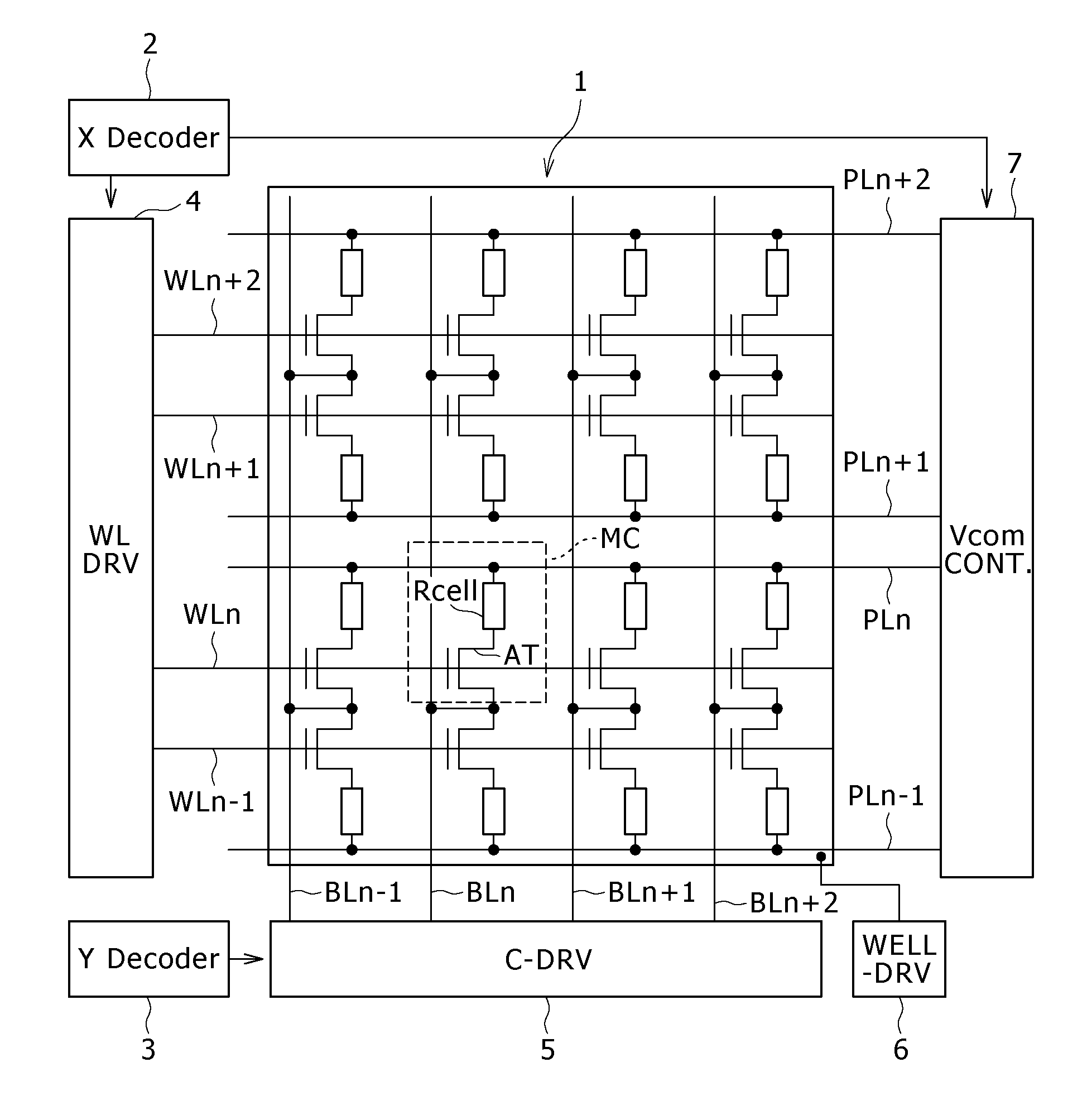
Memory Cell Configuration

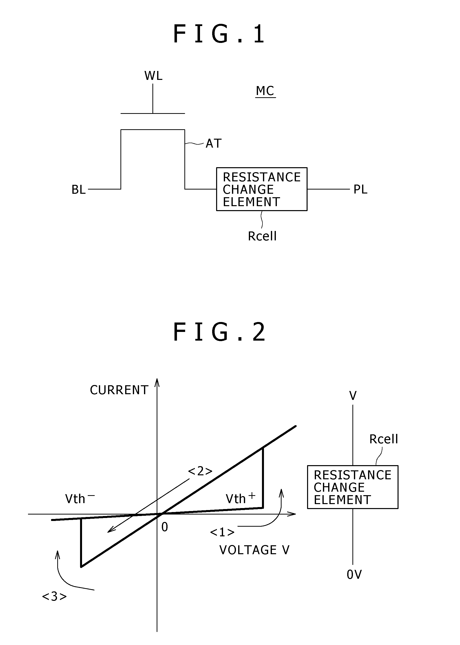
[0041]FIG. 1 is an equivalent circuit diagram of a memory cell according to an embodiment of the present invention.

[0042]A memory cell MC illustrated in FIG. 1 includes a variable cell resistor Rcell and an access transistor AT. The variable cell resistor Rcell serves as a “memory element.”

[0043]The variable cell resistor Rcell has one end connected to a plate line PL, and the other end to the source of the access transistor AT. The access transistor AT has its drain connected to a bit line BL and its gate to a word line WL. The word line WL serves as an “access line.”

[0044]Here, the bit line BL corresponds to an example of a “first wiring,” and the plate line PL to an example of a “second wiring.” Further, the plate line PL may be an example of ...

second embodiment

2. Second Embodiment

[0129]In a second embodiment, a well voltage supply structure is proposed which is effective in providing reduced well resistance for reduced variation in voltage applied to the storage element.

[0130]FIG. 12 illustrates a circuit diagram of the memory cell array according to the second embodiment.

[0131]The memory cell according to the second embodiment differs from that according to the first embodiment shown in FIGS. 6 to 11 in that well bias supply lines WBLx and WBLy shown in FIG. 12 are added. The well bias supply lines WBLx and WBLy are mainly arranged in the x (row) and y (column) directions. At least one of the well bias supply lines WBLx and WBLy is enough to supply a well bias. Here, however, a case is illustrated in which the well bias supply lines are arranged in a grid pattern for the P well 100P.

[0132]The well bias supply lines WBLx and WBLy need only be electrically connected to the P well 100P and include a conductor layer or a conductor region hav...

modification example

3. Modification Example

[0144]The access transistor AT and variable cell resistor Rcell shown in FIG. 1 may be interchanged. That is, the access transistor AT may be connected to the plate line PL, and the variable cell resistor Rcell connected directly to the bit line BL.

[0145]It should be noted, however, that the potential of the bit line BL frequently undergoes a significant change during operation. Therefore, the configuration shown in FIG. 1 is preferred because the effect of such a voltage change can be shut off by the access transistor AT in an OFF state (unselected).

[0146]Further, the set operation (transition from a high to low resistance state) was treated as the write operation, and the reset operation (transition from a low to high resistance state) as the erase operation. However, the set operation may be treated as the erase operation, and the reset operation as the write operation.

[0147]If the access transistor AT is formed with a P-type transistor, an N-type well (N w...


PUM


Abstract

A resistance change memory device includes: memory cells each having a current path in which a storage element, whose resistance changes according to the voltage applied, and an access transistor are connected in series; first wirings each connected to one end of the current path; second wirings each connected to the other end of the current path; a well which is a semiconductor region in which the access transistors are formed; and a drive circuit.

Description

BACKGROUND OF THE INVENTION[0001]1. Field of the Invention[0002]The present invention relates to a resistance change memory device in which each of memory cells is formed by connecting a storage element, whose resistance changes according to the applied voltage, and an access transistor in series, and which is operated by reversing the polarity of a voltage applied to the storage element between data write and erase operations. The present invention also relates to an operation method of the resistance change memory device.[0003]2. Description of the Related Art[0004]Two types of resistance change memory devices are known, one in which a voltage of the same polarity is applied to the storage elements of the memory cells both during data write and erase operations, and another in which the polarity of an applied voltage is reversed between data write and erase operations. The former will be hereinafter referred to as a unipolar voltage-operated resistance change memory, and the latte...

Claims


Application Information

Patent Timeline
IPC IPC(8): G11C11/00
CPCG11C13/0009G11C13/0069G11C2013/0073G11C2213/11G11C2213/34H01L45/1266G11C2213/79H01L27/2436H01L27/2472H01L45/085H01L45/1233G11C2213/56H10B63/82H10B63/30H10N70/245H10N70/8416H10N70/826
Inventor OTSUKA, WATARU
Owner SONY SEMICON SOLUTIONS CORP
Features
  • Generate Ideas
  • Intellectual Property
  • Life Sciences
  • Materials
  • Tech Scout
  • Unparalleled Data Quality
  • Higher Quality Content
  • 60% Fewer Hallucinations
Learn More