Focused ion beam deep nano-patterning apparatus and method

a technology of focused ion beams and nano-patterns, applied in the field of apparatus and method, can solve the problems of low aspect ratio, unwanted metal cut or short circuit, waste of time and crucial chip area, etc., and achieve the effect of high aspect ratio

Active Publication Date: 2010-10-21
TECHNION RES & DEV FOUND LTD
View PDF2 Cites 0 Cited by
  • Summary
  • Abstract
  • Description
  • Claims
  • Application Information

AI Technical Summary

Benefits of technology

[0013]The present invention discloses a high aspect ratio semiconductor nano-patterning technique by focused ion beam. The undesired semiconductor material decomposition by the lower intensity ion beam tail is prevented by a slow-sputter-rate layer forming a funnel and acting effectively as a mask over the semiconductor. The protective layer may be deposited locally allowing nano-scale sputtering with features as smaller than 30 nm and deeper than 350 nm corresponding to aspect ratio higher than 10.

Problems solved by technology

Such low aspect ratio semiconductor milling may cause unwanted metal cuts or short circuits in microelectronics FIB circuit editing (see FIG. 2(a)).
In photonic devices with features as small as few tens of nanometers needed for short-wavelength (visible and UV) applications such low aspect ratios prevent the fabrication of efficient periodic structures.
However, this method wastes time and crucial chip area and, only the predetermined signals can be accessed.

Method used


Image

  • Focused ion beam deep nano-patterning apparatus and method
  • Focused ion beam deep nano-patterning apparatus and method
  • Focused ion beam deep nano-patterning apparatus and method

Examples


Embodiment Construction

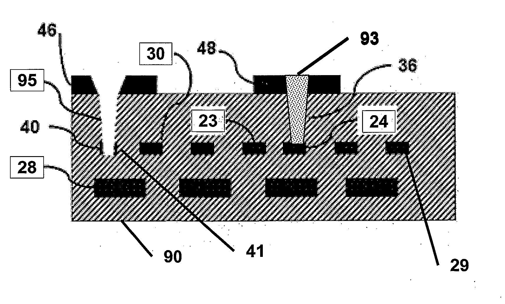
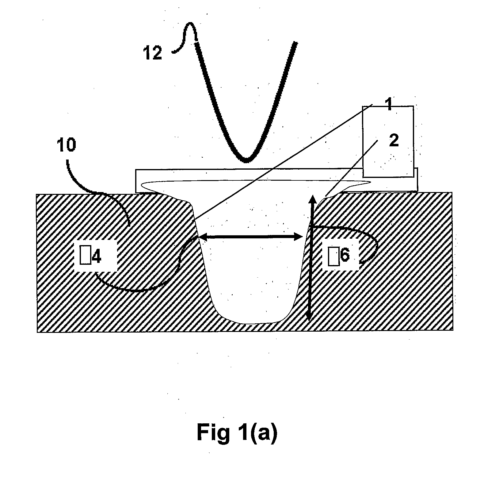
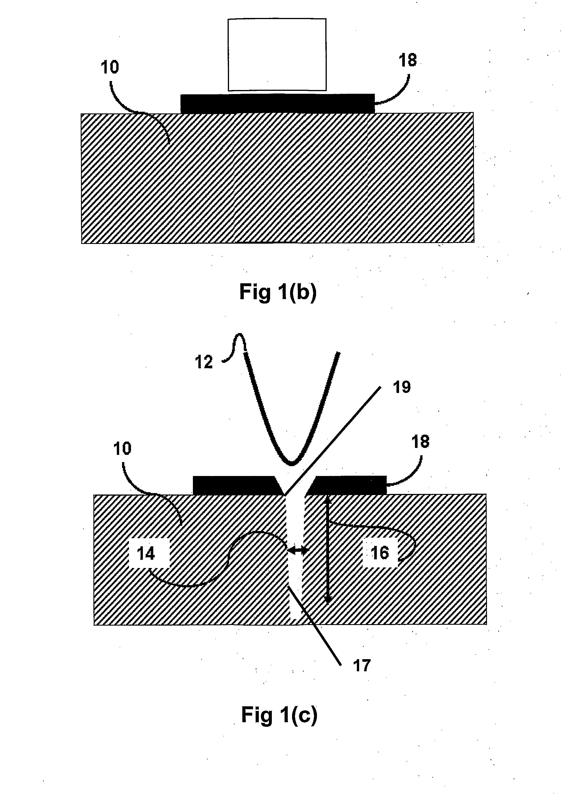
[0048]The present invention relates to an apparatus and method for high aspect-ratio Focused Ion Beam semiconductor nano-patterning wherein undesired semiconductor material decomposition by the beam-tail ions is prevented by a protective Ti layer acting as a mask for the semiconductor.

[0049]Before explaining at least one embodiment of the invention in detail, it is to be understood that the invention is not limited in its application to the details of construction and the arrangement of the components set forth in the following description or illustrated in the drawings. The invention is capable of other embodiments or of being practiced or carried out in various ways. Also, it is to be understood that the phraseology and terminology employed herein is for the purpose of description and should not be regarded as limiting.

[0050]The drawings are generally not to scale. For clarity, non-essential elements were omitted from some of the drawings.

[0051]As used herein, an element or step r...


PUM


Abstract

The present invention introduces a new technique allowing the fabrication of high-aspect ratio nanoscale semiconductor structures and local device modifications using FIB technology. The unwanted semiconductor sputtering in the beam tail region prevented by a thin slow-sputter-rate layer which responds much slower and mostly to the high-intensity ion beam center, thus acting as a saturated absorber funnel-like mask for the semiconductor. The protective layer can be deposited locally using FIB, thus enabling this technique for local device modifications, which is impossible using existing technology. Furthermore, such protective layers allow much higher resolution and nanoscale milling can be achieved with very high aspect ratios, e.g. Ti layer results in aspect ratio higher than 10 versus bare semiconductor milling ratio of about 3.

Description

FIELD OF THE INVENTION[0001]The present invention relates to an apparatus and method for high aspect-ratio Focused Ion Beam semiconductor nano-patterning wherein undesired semiconductor material decomposition by the beam-tail ions is prevented by a protective Ti layer acting as a mask for the semiconductor.BACKGROUND OF THE INVENTION[0002]Focused ion beam (FIB) etching has been widely used as a versatile maskless lithography technique in numerous fields. Nano-patterning using FIB etching is generally employed in order to develop or locally modify devices, including integrated circuits, micro-systems and micro-photonics. Due to the ability of FIB patterning to save time and process steps, it can be exploited to develop prototypes of both electrical and optical devices: Many photonic and optoelectronic devices employ sub-wavelength-scale structures, such as diffraction gratings, Distributed Bragg reflectors (DBRs), photonic crystals, and surface plasmon devices.[0003]In semiconductors...

Claims


Application Information

Patent Timeline
Patent Type & Authority Applications(United States)
IPC IPC(8): H01L21/768
CPCB81C1/00063H01L21/3065H01L21/32131H01L21/3085H01L21/3081
Inventor HAYAT, ALEXLAHAV, ALEXORENSTEIN, MEIR
Owner TECHNION RES & DEV FOUND LTD
Why Eureka
Try Eureka