Correction of aging in amoled display

a technology of amoled display and display panel, which is applied in the direction of instruments, static indicating devices, etc., can solve the problems of low accuracy, low cost, and limited number of lines of current-sourced drive electronics

Inactive Publication Date: 2010-11-04
SILICONFILE TECH INC
View PDF14 Cites 229 Cited by
  • Summary
  • Abstract
  • Description
  • Claims
  • Application Information

AI Technical Summary

Problems solved by technology

While PM OLEDs are fairly simple structures to design and fabricate, they demand relatively expensive, current-sourced drive electronics to operate effectively and are limited as to the number of lines because only one line can be on at a time and therefore the PM OLED must have instantaneous brightness equal to the desired average brightness times the number of lines.
Thus, PM OLED displays are typically limited to under 100 lines.
In addition, their power consumption is significantly higher than that required by an active-matrix OLED.
However, the TFTs in the AMOLED are typically fabricated with poly-silicon (p-Si) that is difficult to fabricate in a uniform manner.
Unfortunately the grain size produced in the laser anneal step is not uniform due to a temperature spread in the laser b...

Method used


Image

  • Correction of aging in amoled display
  • Correction of aging in amoled display
  • Correction of aging in amoled display

Examples


Embodiment Construction

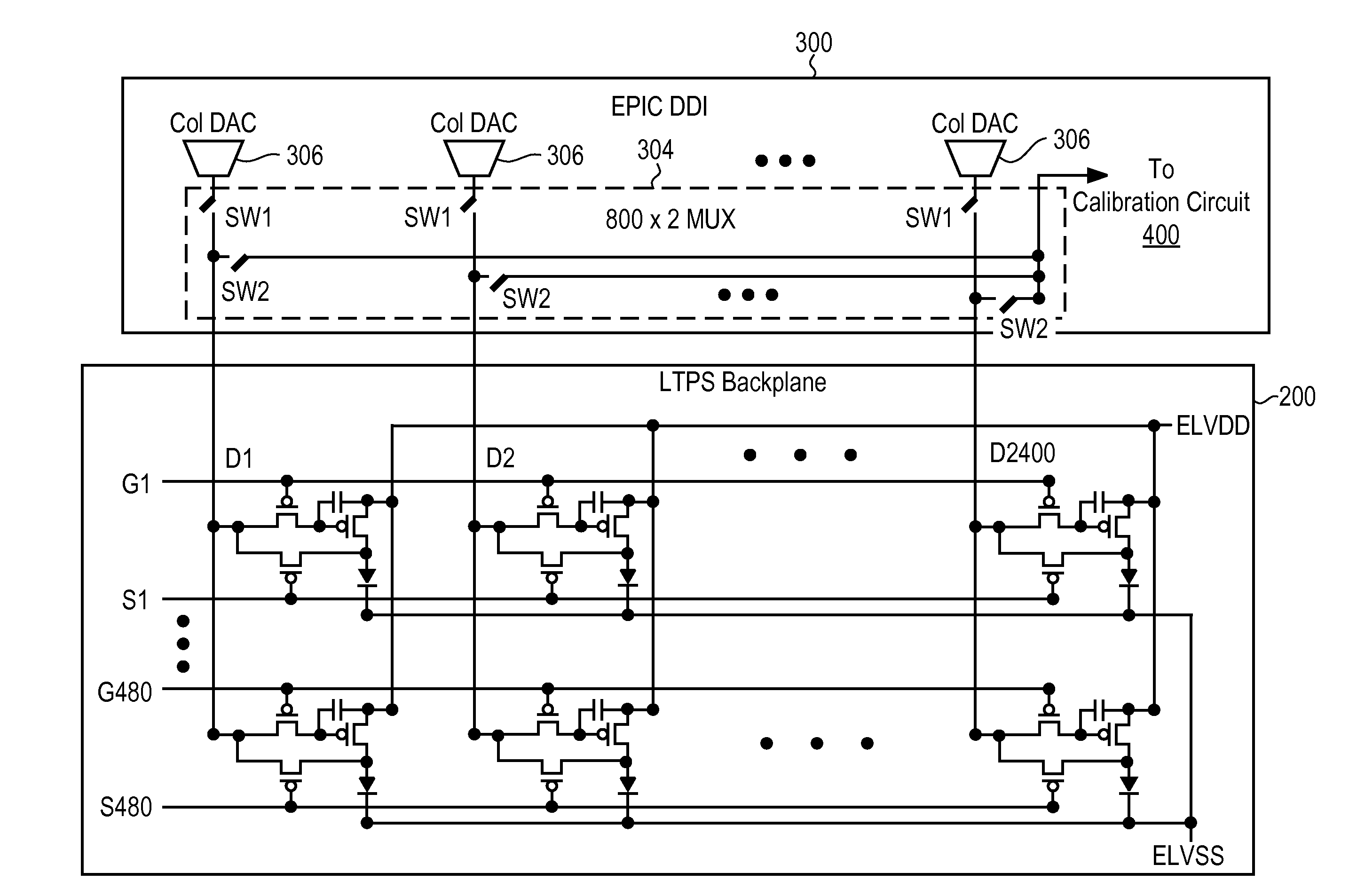
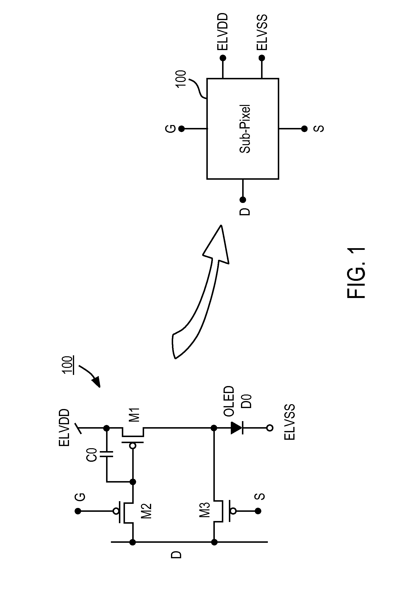
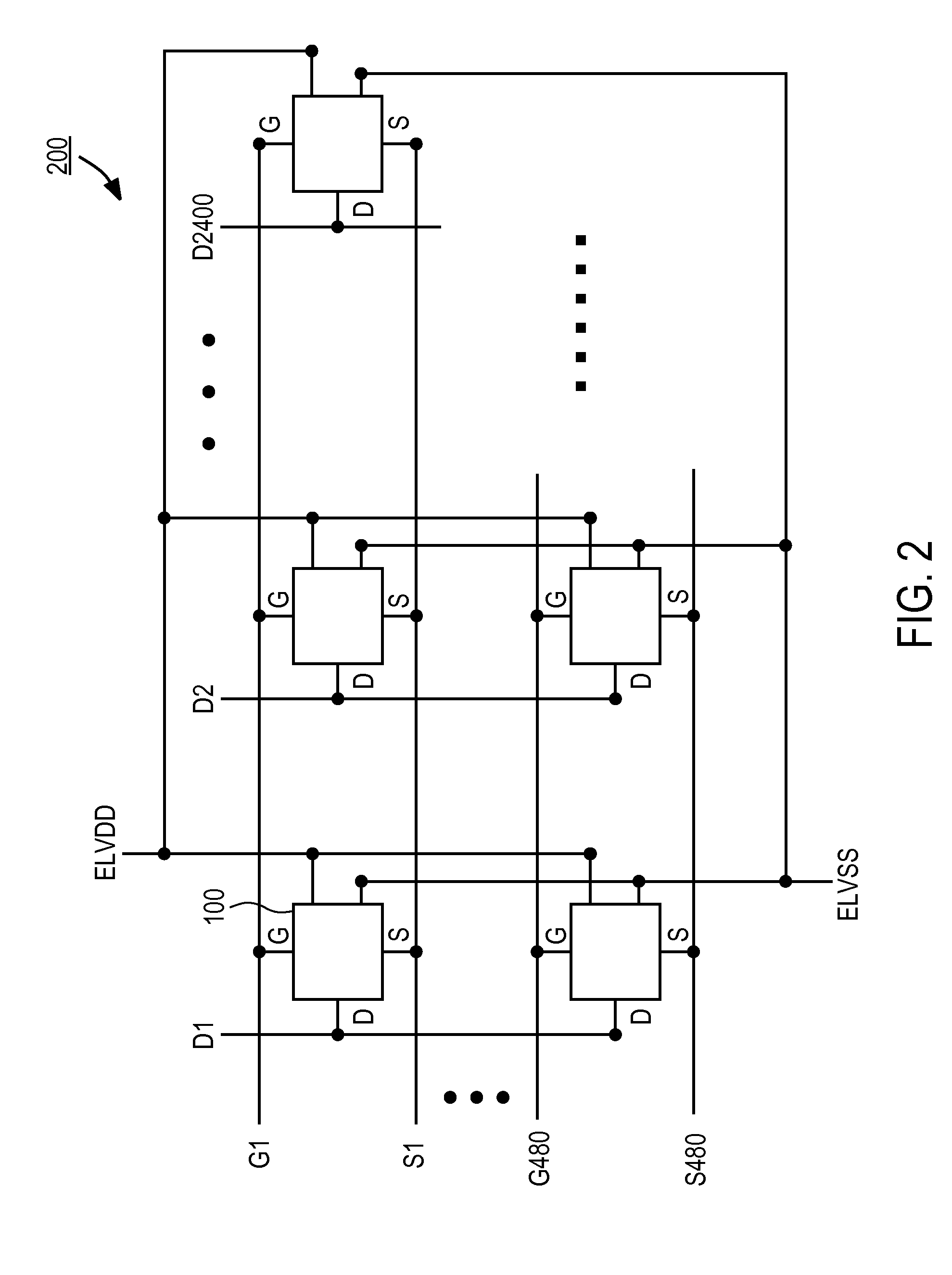
[0022]The Figures and the following description relate to preferred embodiments of the present invention by way of illustration only. It should be noted that from the following discussion, alternative embodiments of the structures and methods disclosed herein will be readily recognized as viable alternatives that may be employed without departing from the principles of the claimed invention.

[0023]Reference will now be made in detail to several embodiments of the present invention(s), examples of which are illustrated in the accompanying figures. It is noted that wherever practicable similar or like reference numbers may be used in the figures and may indicate similar or like functionality. The figures depict embodiments of the present invention for purposes of illustration only. One skilled in the art will readily recognize from the following description that alternative embodiments of the structures and methods illustrated herein may be employed without departing from the principle...


PUM


Abstract

The data line voltage on the data line of the AMOLED sub-pixels is measured while the OLED is being driven by a reference current, in order to determine the age of the OLED in the sub-pixel. The pixel transistor serves as a current source for driving the OLED in the sub-pixel with the reference current. The data line voltage is substantially equal to the forward voltage VF(aged) of the aged OLED being driven at the reference current. The forward voltage VF (un-aged) of a reference (un-aged) OLED sub-pixel also measured at the reference current, and is subtracted from the measured OLED diode forward voltage VF (aged) to obtain their difference ΔVF=VF(aged)−VF(un-aged). ΔVF is an indicator of the age of the OLED in the sub-pixel, and is used as an index to a look-up-table that stores the corresponding aging offset data for generating the incremental pixel current needed to maintain constant luminance in the aged OLED pixel.

Description

BACKGROUND OF THE INVENTION[0001]1. Field of the Invention[0002]The present invention relates to calibration of current variations in the pixels / sub-pixels of an active matrix organic light-emitting diode (AMOLED) display caused by aging of the organic light-emitting diodes (OLEDs) in the AMOLED sub-pixels.[0003]2. Description of the Related Arts[0004]An OLED display is generally comprised of an array of organic light emitting diodes (hereafter referred to as “OLED diodes”) that have carbon-based films deposited between two charged electrodes. Generally one electrode is comprised of a transparent conductor, for example, indium tin oxide (ITO). Generally, the organic material films are comprised of a hole-injection layer, a hole-transport layer, an emissive layer and an electron-transport layer. When voltage is applied to the OLED diode, the injected positive and negative charges recombine in the emissive layer and transduce electrical energy to light energy. Unlike liquid crystal di...

Claims


Application Information

Patent Timeline
IPC IPC(8): G09G3/30
CPCG09G3/3275G09G2300/0819G09G2300/0842G09G2310/027G09G2310/0297G09G2370/08G09G2320/029G09G2320/043G09G2320/048G09G2320/0693G09G2320/0285G09G2320/045
Inventor JEONG, KOANYEL
Owner SILICONFILE TECH INC
Why Eureka
Try Eureka