Semiconductor device

a technology of semiconductor devices and semiconductor parts, applied in semiconductor devices, semiconductor/solid-state device details, electrical devices, etc., can solve the problems of deterioration of bonding reliability and bonding defects at the above-mentioned bonding portions, and achieve the effect of reducing the size of a semiconductor devi

Active Publication Date: 2010-12-02
RENESAS ELECTRONICS CORP
View PDF5 Cites 97 Cited by
  • Summary
  • Abstract
  • Description
  • Claims
  • Application Information

AI Technical Summary

Benefits of technology

[0006]For attaining high speed, high function and reduction of size of a semiconductor device, a so-called flip-chip mounting method is considered to be effective wherein a semiconductor chip with electrode pads formed thereon is mounted onto a wiring substrate in such a manner that a main surface of the semiconductor chip confronts a main surface of the wiring substrate as a substrate for mounting the semiconductor chip.
[0011]In view of this problem the present inventors have made a study about increasing the temperature of the tool and that of the stage. As a result, the wettability of the soldering material for the bump electrodes not surrounded by other bump electrodes was improved, but it was found that a crack was developed in an insulating film formed between a bump electrode-disposed pad with few heat dissipating paths and a corresponding cell.
[0012]In this connection the present inventors have made a study about a configuration wherein dummy bumps functioning as heat retaining walls are disposed in gaps and ends of a bump electrode array to suppress variations in temperature between bump electrodes.
[0014]The present invention has been accomplished in view of the above-mentioned problems and it is an object of the invention to provide a technique able to improve the reliability of a semiconductor device.
[0019]It is possible to reduce the size of a semiconductor device.

Problems solved by technology

Therefore, if the temperature applied to each bonding portion is low, the soldering material becomes difficult to wet and rise onto the bump electrode, with consequent deterioration of the bonding reliability.
This time, the present inventors mounted a semiconductor chip onto a wiring substrate with use of such a flip-chip mounting method and found that bonding defects occurred at the aforesaid bonding portions.
Having examined this problem, we found that the problem was caused by a non-uniform layout of the bump electrodes formed on the semiconductor chip to be mounted onto the wiring substrate.

Method used


Image

  • Semiconductor device
  • Semiconductor device
  • Semiconductor device

Examples


Embodiment Construction

Explanation of Description Form, Basic Terms and how to Use

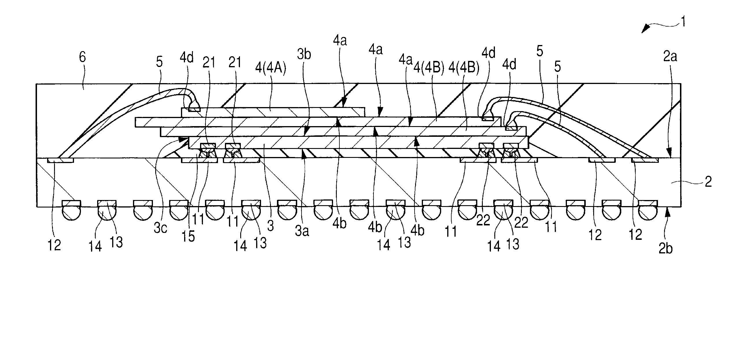
[0054]An embodiment of the present invention will be described dividedly into plural sections or the like where required for convenience' sake, but unless otherwise mentioned, it is to be understood that the divided sections are not independent of each other, but configure portions of a single example, or in a relation such that one is a partial detail of the other or is a modification of part or the whole of the other, irrespective of whether the description of one is before or after the description of the other. As to similar portions, repeated explanations thereof are omitted in principle. Constituent elements in an embodiment are not essential unless otherwise mentioned and except the case where they are limited theoretically to specified numbers thereof, further, except the case where they are clearly essential contestually.

[0055]Likewise, in the description of an embodiment or the like, as to “X comprising A” or the li...


PUM


Abstract

The reliability of a semiconductor device is to be improved. A microcomputer chip (semiconductor chip) having a plurality of pads formed on a main surface thereof is mounted over an upper surface of a wiring substrate in an opposed state of the chip main surface to the substrate upper surface. Pads coupled to a plurality of terminals (bonding leads) formed over the substrate upper surface comprise a plurality of first pads in which a unique electric current different from the electric current flowing through other pads flows and a plurality of second pads in which an electric current common to the pads flows or does not flow. Another first pad of the first pads or one of the second pads are arranged next to the first pad. The first pads are electrically coupled to a plurality of bonding leads respectively via a plurality of bumps (first conductive members), while the second pads are bonded to the terminals via a plurality of bumps (second conductive members).

Description

CROSS-REFERENCE TO RELATED APPLICATIONS[0001]The disclosure of Japanese Patent Application No. 2009-130804 filed on May 29, 2009 including the specification, drawings and abstract is incorporated herein by reference in its entirety.BACKGROUND OF THE INVENTION[0002]The present invention relates to a technique of a semiconductor device, particularly a technique applicable effectively to a semiconductor device wherein a semiconductor chip with electrode pads formed thereon is mounted onto a wiring substrate in a state in which its main surface is opposed to a chip mounting surface of the wiring substrate.[0003]In connection with a semiconductor device package there is known a technique wherein a semiconductor chip is flip-chip-mounted onto a wiring substrate. For example, in Japanese Unexamined Patent Publication No. 2003-100801 (Patent Document 1) and No. 2008-218758 (Patent Document 2) is described a so-called flip-chip mounting type semiconductor device wherein a semiconductor chip ...

Claims


Application Information

Patent Timeline
Patent Type & Authority Applications(United States)
IPC IPC(8): H01L23/522H01L23/52H01L23/538
CPCH01L21/563H01L23/3128H01L23/5226H01L23/5283H01L23/5286H01L24/05H01L24/06H01L24/13H01L24/14H01L24/16H01L24/45H01L24/48H01L24/49H01L24/81H01L24/97H01L25/0657H01L25/18H01L2224/0401H01L2224/05599H01L2224/06515H01L2224/1134H01L2224/13144H01L2224/14515H01L2224/32145H01L2224/45144H01L2224/48091H01L2224/48227H01L2224/48465H01L2224/49171H01L2224/49175H01L2224/4943H01L2224/73203H01L2224/81193H01L2224/81203H01L2224/81801H01L2224/83102H01L2224/92125H01L2224/97H01L2225/0651H01L2225/06517H01L2225/06562H01L2924/01004H01L2924/01014H01L2924/01028H01L2924/01029H01L2924/01047H01L2924/0105H01L2924/01078H01L2924/01079H01L2924/01082H01L2924/01083H01L2924/014H01L2924/14H01L2924/15311H01L2924/30107H01L2924/3011H01L2924/01005H01L2924/01006H01L2924/01033H01L2224/16225H01L2224/32225H01L2224/73204H01L2224/73265H01L2924/00014H01L2224/48599H01L2224/04042H01L2224/05553H01L2224/02166H01L2224/85H01L2224/83H01L2224/81H01L2924/00012H01L2924/00H01L2224/92247H01L2924/181H01L24/73H01L2224/05093H01L2924/15184H01L2224/49433
Inventor TAOKA, NAOTONAKAMURA, ATSUSHIMORINO, NAOZUMIISHIKAWA, TOSHIKAZUKINOSHITA, NOBUHIRO
Owner RENESAS ELECTRONICS CORP
Why Eureka
Try Eureka