Memory device and methods for fabricating and operating the same

a memory device and memory technology, applied in the field of memory devices, can solve the problems of easy leakage of leakage information in the device, prone to worse programming disturbance, and compromise of device reliability

Active Publication Date: 2010-12-02
MACRONIX INT CO LTD
View PDF6 Cites 4 Cited by
  • Summary
  • Abstract
  • Description
  • Claims
  • Application Information

AI Technical Summary

Benefits of technology

[0009]Accordingly, the present invention is directed to a memory device capable of increasing the number of bits in a unit cell.
[0036]As mentioned above, the memory device in the present invention includes a planar channel cell and a vertical channel cell, such that six physical bits are used for storing data in a single memory cell. Accordingly, the bit density can be increased, and the storage density is also enhanced without affecting the layout size.
[0037]Besides, the method for fabricating the memory device in the present invention forms the first doped regions adjacent to the upper portion of each trench and also forms the second doped regions under the bottoms of the trenches. Hence, the memory device to be formed can have a structure of 6-bit-per-cell with an enhance storage density.
[0038]Additionally, the method for operating the memory device in the present invention stores the electrons into the respective six bits of each memory cell for programming, and also injected the holes thereinto for erasing. Thus, the storage density is improved without mutual perturbation and programming disturbance.

Problems solved by technology

However, when there are defects in the tunnel oxide layer under the polysilicon floating gate, the leakage is easily produced in the device.
Hence, the reliability of the device is compromised.
When the cell length is scaled down, the planar channel cell is prone to worse programming disturbance and higher resistance of the source and drain regions.
However, the electrons punch through easily between two bottom junctions, and the leakage in the memory structure is induced severely.
The programming disturbance usually occurs due to the close deployment of neighboring trenches.

Method used


Image

  • Memory device and methods for fabricating and operating the same
  • Memory device and methods for fabricating and operating the same
  • Memory device and methods for fabricating and operating the same

Examples


Embodiment Construction

[0053]Reference will now be made in detail to the present preferred embodiments of the invention, examples of which are illustrated in the accompanying drawings. Wherever possible, the same reference numbers are used in the drawings and the description to refer to the same or like parts.

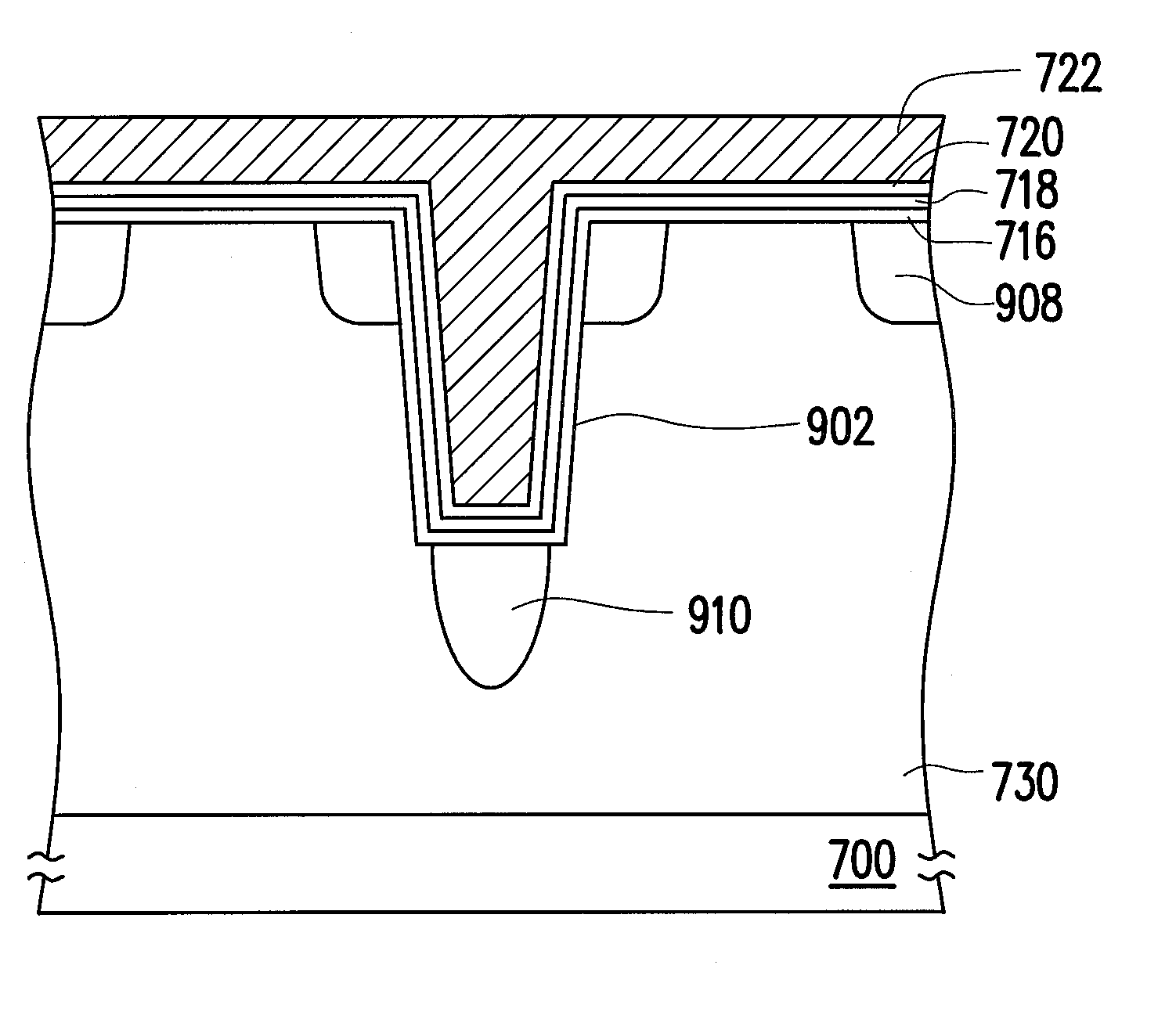
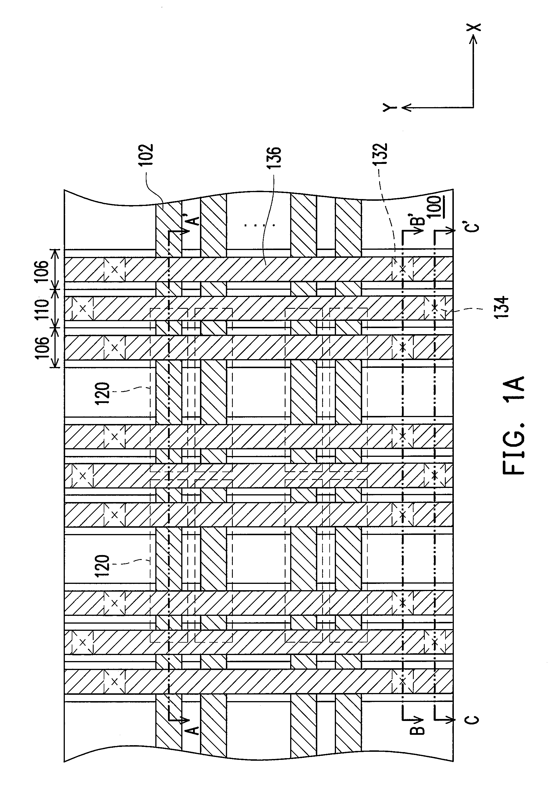
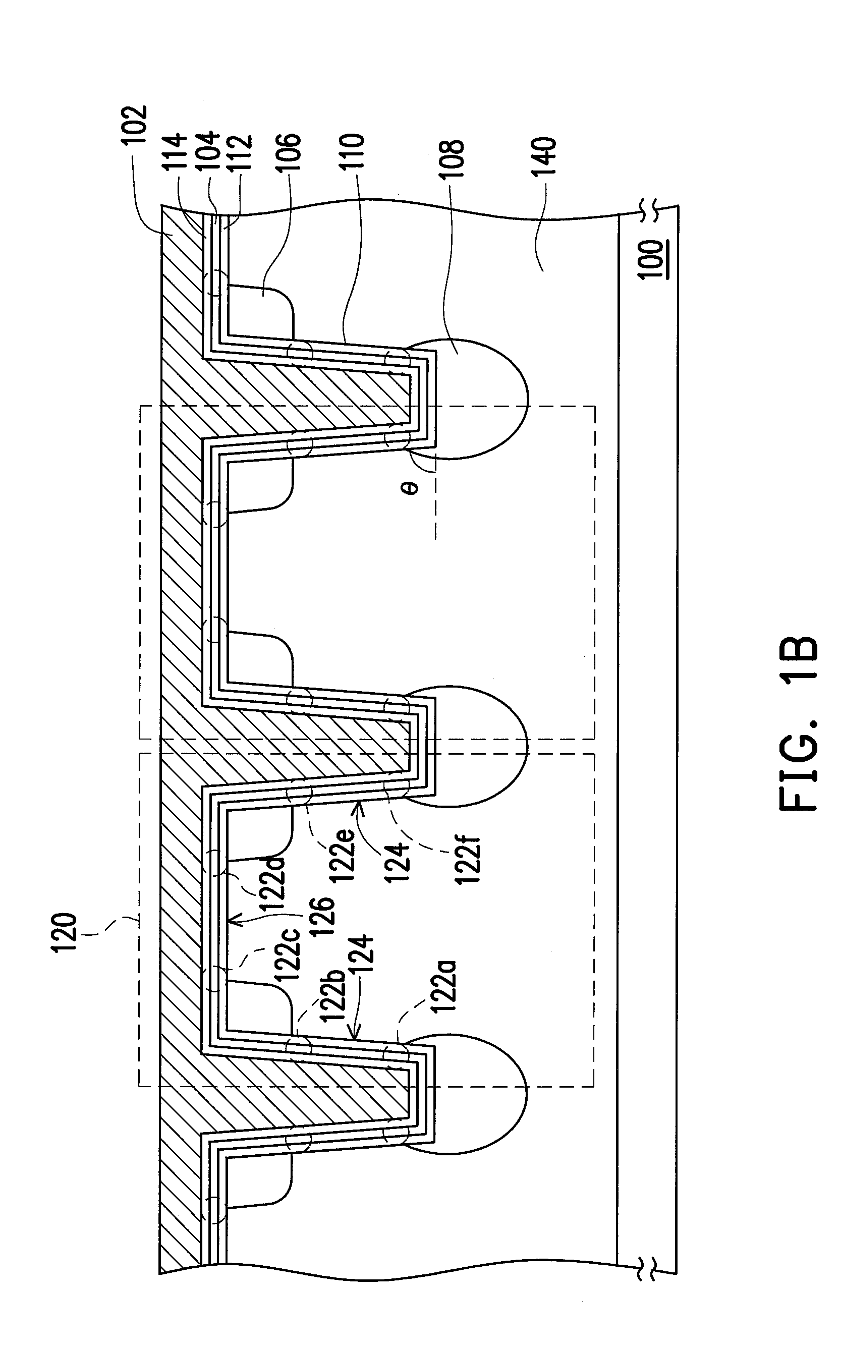
[0054]FIG. 1A schematically illustrates a top view layout of the memory device according to an embodiment of the present invention, in which the inter-layer dielectric (ILD) is hidden. FIG. 1B is schematic, cross-sectional diagram of the memory device shown in FIG. 1A along line A-A′ according to an embodiment of the present invention. FIG. 1C is schematic, cross-sectional diagram of the memory device shown in FIG. 1A along line B-B′ according to an embodiment of the present invention. FIG. 1D is schematic, cross-sectional diagram of the memory device shown in FIG. 1A along line C-C′ according to an embodiment of the present invention. FIG. 2 is schematic, cross-sectional diagram of the memory device...


PUM


Abstract

The memory device is described, which includes a substrate, a conductive layer, a charge storage layer, a plurality of first doped regions and a plurality of second doped regions. The substrate has a plurality of trenches formed therein. The conductive layer is disposed on the substrate and fills the trenches. The charge storage layer is disposed between the substrate and the conductive layer. The first doped regions are configured in the substrate adjacent to both sides of an upper portion of each trench, respectively. The first doped regions between the neighbouring trenches are separated from each other. The second doped regions are configured in the substrate under bottoms of the trenches, respectively. The second doped regions and the first doped regions are separated from each other, such that each memory cell includes six physical bits.

Description

BACKGROUND OF THE INVENTION[0001]1. Field of the Invention[0002]The present invention generally relates to a semiconductor device. More particularly, the present invention relates to a memory device, and to a fabricating method and an operating method of the same.[0003]2. Description of Related Art[0004]A memory is a semiconductor device designed for storing information or data. As the functions of computer microprocessors become more and more powerful, programs and operations executed by software are increasing correspondingly. Consequentially, the demand for high storage capacity memories is getting more. Among various types of memory products, a non-volatile memory allows multiple-time data programming, reading and erasing operations, and the data stored therein can be retained even after the power to the memory is terminated. With these advantages, the non-volatile memory has become one of the most widely adopted memories for personal computers and electronic equipment.[0005]Ele...

Claims


Application Information

Patent Timeline
Patent Type & Authority Applications(United States)
IPC IPC(8): G11C16/04H01L29/792H01L21/28
CPCG11C16/0475H01L27/11521H01L27/11568H10B41/30H10B43/30
Inventor YANG, I-CHENWU, GUAN-WEICHEN, PO-CHOUCHANG, YAO-WENLU, TAO-CHENG
Owner MACRONIX INT CO LTD
Why Eureka
Try Eureka