Fine-structure transfer apparatus

a technology of nano-imprinting and transfer apparatus, which is applied in the direction of dough shaping, manufacturing tools, food shaping, etc., can solve the problems of marked drop in throughput, inability to create fine structures smaller than the wavelength of light, and inconvenient photolithography, so as to improve efficiency, eliminate transfer defects, and facilitate the effect of production

Inactive Publication Date: 2010-12-02
HITACHI HIGH-TECH CORP
View PDF9 Cites 14 Cited by
  • Summary
  • Abstract
  • Description
  • Claims
  • Application Information

AI Technical Summary

Benefits of technology

[0026]In the fine-structure transfer apparatus according to the first aspect of the present invention, a flexible stamper is rendered to have an elongated structure and by fixing one of its end while designing the other end to be vertically movable, the stamper can be deformed into a curved shape so that the entire surface of the transfer element is gradually covered with the curved stamper, starting from its outer periphery and directed radially towards its center. As a result, the air present at the interface between the stamper and the transfer element will be pushed to the outside of the interface as the transfer element is being covered with the stamper, ensuring that no air will be left at the interface. This substantially eliminates transfer defects that would otherwise occur on account of air bubbles in the conventional fine-structure transfer apparatus. When the transfer step is over, the stamper is gradually detached fro

Problems solved by technology

Conventional photolithography which uses the exposure process is capable of microfabrication over a large area in one step; however, since its resolution is not finer than the wavelength of light, conventional photolithography is inevitably unsuitable for creating fine structures smaller than the wavelength of light (say, 100 nm and less).
Therefore, as the recording density increases, the time it takes to form a fine-featured pattern is prolonged to cause a marked drop in throughput.
With a view to forming patterns at a faster speed by the e-beam lithographic equipment, the development of a method for one-shot irradiation of geometric figures is underway in which combinations of variously shaped masks are subjected to one-shot exposure to electron beams; however, the e-beam lithographic apparatus that uses the method for one-shot irradiation of geometric figures is not only bulky but it also needs an additional mechanism for controllin

Method used


Image

  • Fine-structure transfer apparatus
  • Fine-structure transfer apparatus
  • Fine-structure transfer apparatus

Examples


Embodiment Construction

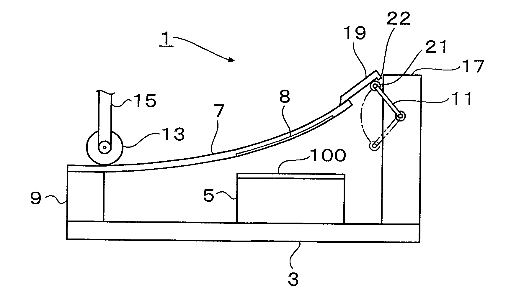
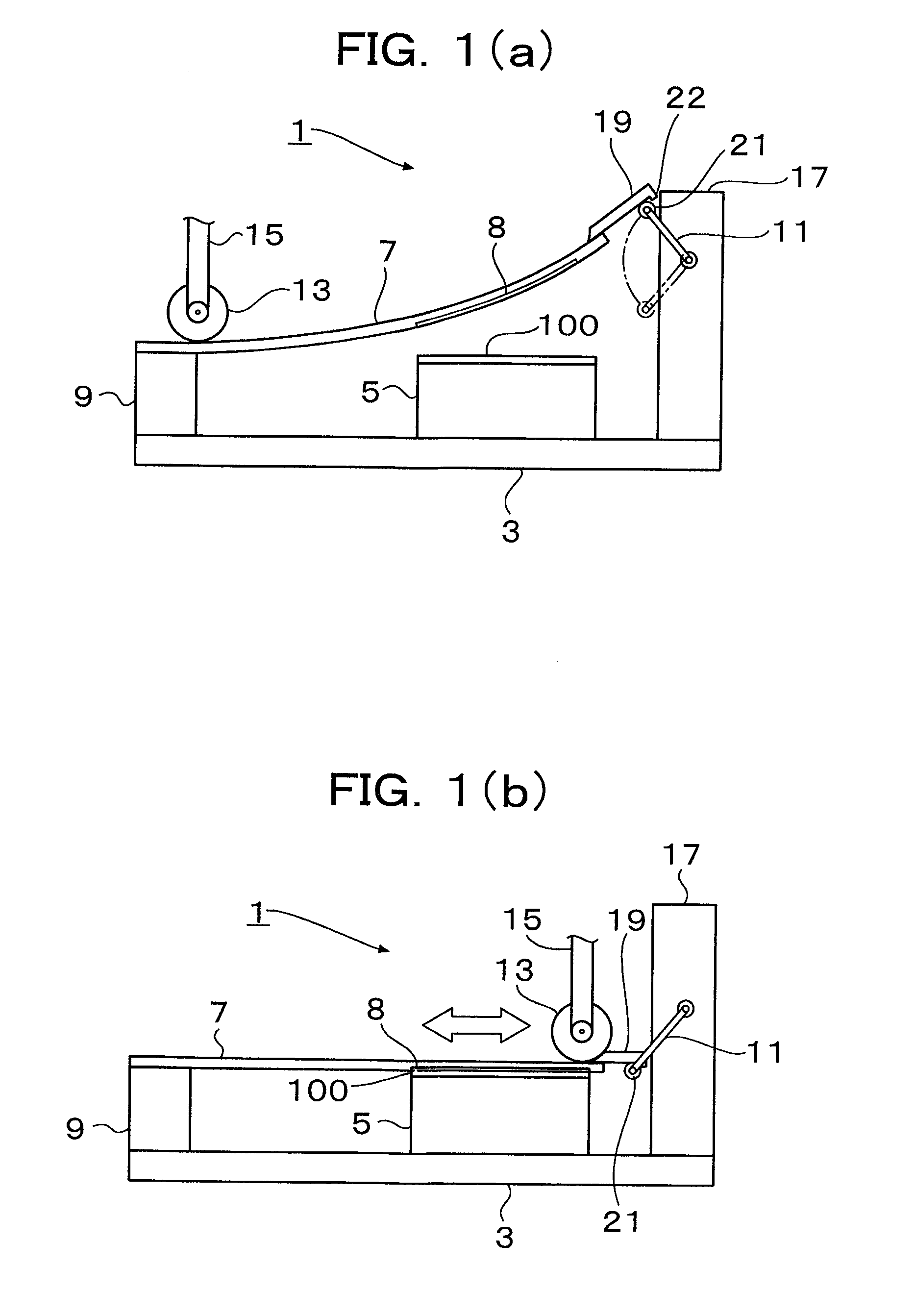
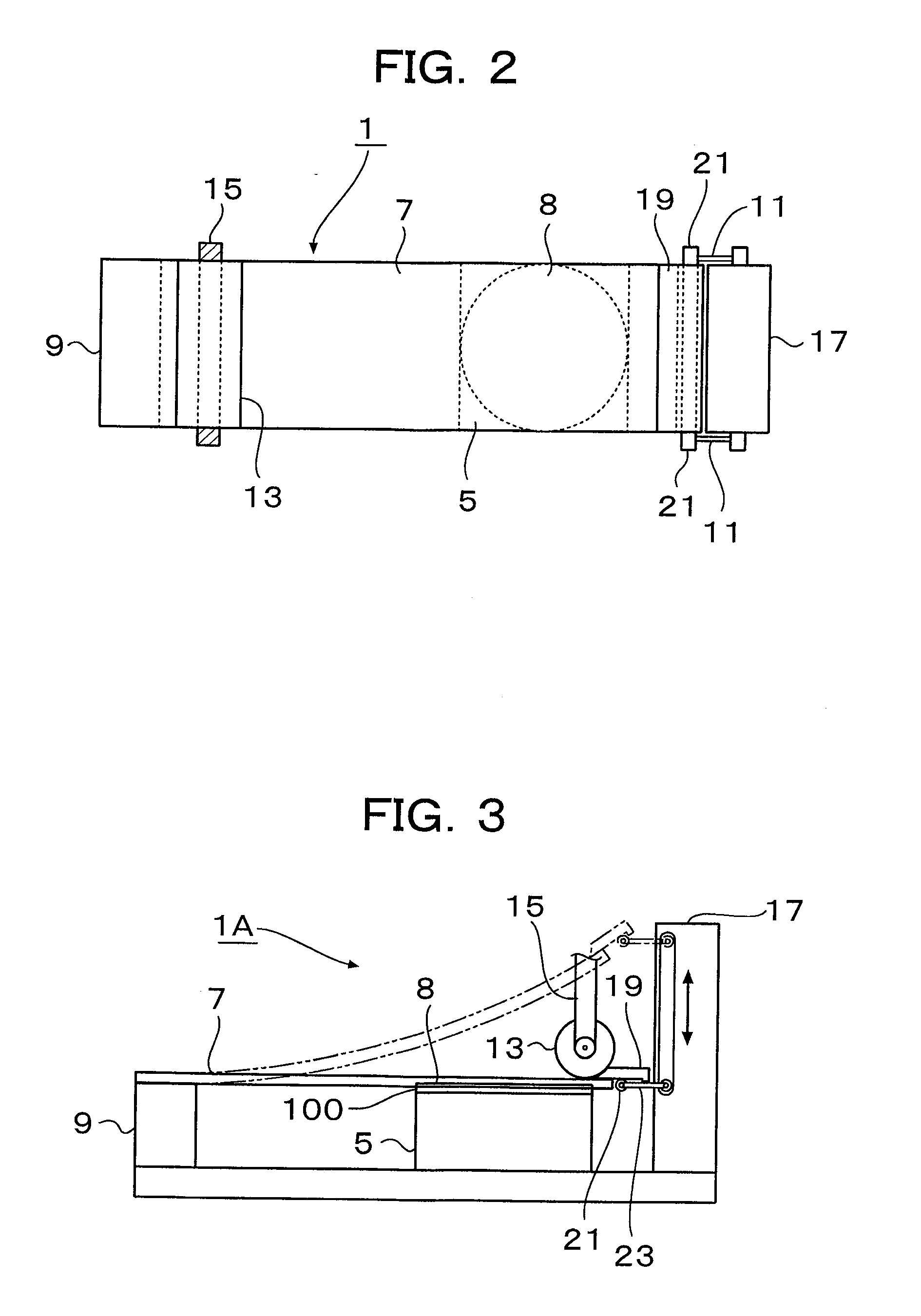
[0040]FIG. 1(a) is a front view showing an outline of an embodiment of the fine-structure transfer apparatus according to the first aspect of the present invention, before pressure is applied to a stamper. FIG. 1(b) is a front view showing the same, with pressure applied to the stamper. FIG. 2 is a plan view of the fine-structure transfer apparatus shown in FIG. 1. The fine-structure transfer apparatus of the present invention which is generally indicated by 1 has the following basic components: a base plate 3, a stage 5 placed on top of the base plate 3 for holding a transfer element 100 in position, and a stamper 7 provided over the stage 5. The stamper 7 is elongated in shape; one of its ends is fixed to a first post 9 and the other end can be lifted upward like a cantilevered spring by means of a pivoting arm 11 that reciprocates in a vertical direction. The pivoting arm 11 is mounted on a second post 17 in such a way that by means of a suitable cam mechanism not shown, it can p...


PUM

PropertyMeasurementUnit
Pressureaaaaaaaaaa
Angleaaaaaaaaaa
Flexibilityaaaaaaaaaa

Abstract

A fine-structure transfer apparatus has a base plate, a first post and a second post erected on the upper surface of the base plate, an elongated stamper that is fixed at one end to the upper end face of the first post. The stamper is supported at the other end in a vertically movable manner by means of an ascending/descending unit provided on the second post. A transfer element holding stage is provided on the upper surface of the base plate between the first and second posts in a position that corresponds to the position of the lower surface of the elongated stamper where a fine pattern is formed. A pressure-applying unit is provided to reciprocate on the upper surface of the elongated stamper along a longitudinal direction thereof. The transfer apparatus is characterized by the ease with which the stamper can be detached from the transfer element.

Description

TECHNICAL FIELD[0001]The present invention relates to a fine-structure transfer or nanoimprint apparatus. More particularly, the present invention relates to a fine-structure transfer or nanoimprint apparatus that not only allows a stamper to be easily attached to and detached from a transfer element but also effectively prevents the occurrence of air bubbles as a transfer defect.BACKGROUND ART[0002]With remarkable advances in the performance of computers and other information equipment, the volume of information that is handled by users has been constantly increasing and the unit of measurement is now in terabytes rather than gigabytes. Under these circumstances, there exists an ever-growing demand for semiconductor devices such as information storage / reproduce equipment and memories that are capable of recording at even higher densities.[0003]To achieve higher recording densities, technologies for even finer microfabrication are required. Conventional photolithography which uses t...

Claims


Application Information

Patent Timeline
IPC IPC(8): B29C59/02
CPCB29C35/0888B29C37/0003B29C37/006B29C43/021B29C43/06B29C43/3697B29C59/022B29C2035/0827B29C2043/025B29C2059/023
Inventor MORI, KYOICHISHIZAWA, NORITAKEYAMASHITA, NAOAKITSUSHIMA, KOJISHIRAISHI, TOSHIMITSU
Owner HITACHI HIGH-TECH CORP
Why Eureka
Try Eureka