Thin Film Interference Filter and Bootstrap Method for Interference Filter Thin Film Deposition Process Control

a thin film deposition process and interference filter technology, applied in the field of complex interference filters, can solve the problems of large amount of optical dielectric, e.g., greater than ten microns, and high manufacturing tolerances and costs of bulk optical dielectrics, and achieve unpredictable, irregular, irregular, or otherwise undesirable passbands

Active Publication Date: 2010-12-02
HALLIBURTON ENERGY SERVICES INC
View PDF100 Cites 50 Cited by
  • Summary
  • Abstract
  • Description
  • Claims
  • Application Information

AI Technical Summary

Benefits of technology

[0014]In general, the present invention is directed to a layered, thin film interference filter and related bootstrap methods. A bootstrap method according to one aspect of the invention permits a user to focus on a single layer of a film stack as the layer is deposited to obtain an estimate of the properties of the stack. Although the single layer model is a guideline and not a basis for compensating errors, only the most-recently-deposited layer—and not the already-deposited film stack—need be modeled according to an aspect of the present invention. Thus, the user can neglect deviations of the stack from ideality for all other layers. The single-layer model can then be fit exactly to the observed spectra of the film stack at each stage of deposition to allow accurate updating of the remaining film stack for continued deposition.
[0015]The present invention works with any type of films, whether absorbing or non-absorbing, and regardless of whether the control of the deposition conditions are state-of-the-art or not. The methods of the invention are relatively straightforward, and a resultant thin film interference filter is economical to produce and use.

Problems solved by technology

A design that requires very tight manufacturing tolerances over large substrate areas could result in the costly rejection of many devices.
A bulk optical dielectric, e.g., greater than ten microns, disposed between metal or dielectric mirrors suffers from excessive manufacturing tolerances and costs.
Moreover, the bulk material provides unpredictable, imprecise, irregular, or otherwise undesirable passbands.
These electrical and mechanical optical filters disadvantageously do not provide precise rejection bands and passbands that are repeatably manufactured.
However, films vary in ways that cannot be readily modelled using any fixed or simple physical model.
Heterogeneities in the films that cannot be predicted or compensated by this method cause the observed spectra to deviate more and more from the model.
This makes continued automatic deposition very difficult; complex film stacks are therefore very operator-intensive and have a high failure rate.
As outlined above, many thin films are usually designed in a stack to produce complex spectra and small variations in deposition conditions make it difficult to accurately model in situ film spectra for feedback control of a continuous deposition process because it is practically impossible to obtain full knowledge of the detailed structure of the stack from reflectance, transmittance, ellipsometry, mass balance or other methods.

Method used


Image

  • Thin Film Interference Filter and Bootstrap Method for Interference Filter Thin Film Deposition Process Control
  • Thin Film Interference Filter and Bootstrap Method for Interference Filter Thin Film Deposition Process Control
  • Thin Film Interference Filter and Bootstrap Method for Interference Filter Thin Film Deposition Process Control

Examples


Embodiment Construction

[0042]Detailed reference will now be made to the drawings in which examples embodying the present invention are shown. Repeat use of reference characters in the drawings and detailed description is intended to represent like or analogous features or elements of the present invention.

[0043]The drawings and detailed description provide a full and detailed written description of the invention and the manner and process of making and using it, so as to enable one skilled in the pertinent art to make and use it. The drawings and detailed description also provide the best mode of carrying out the invention. However, the examples set forth herein are provided by way of explanation of the invention and are not meant as limitations of the invention. The present invention thus includes modifications and variations of the following examples as come within the scope of the appended claims and their equivalents.

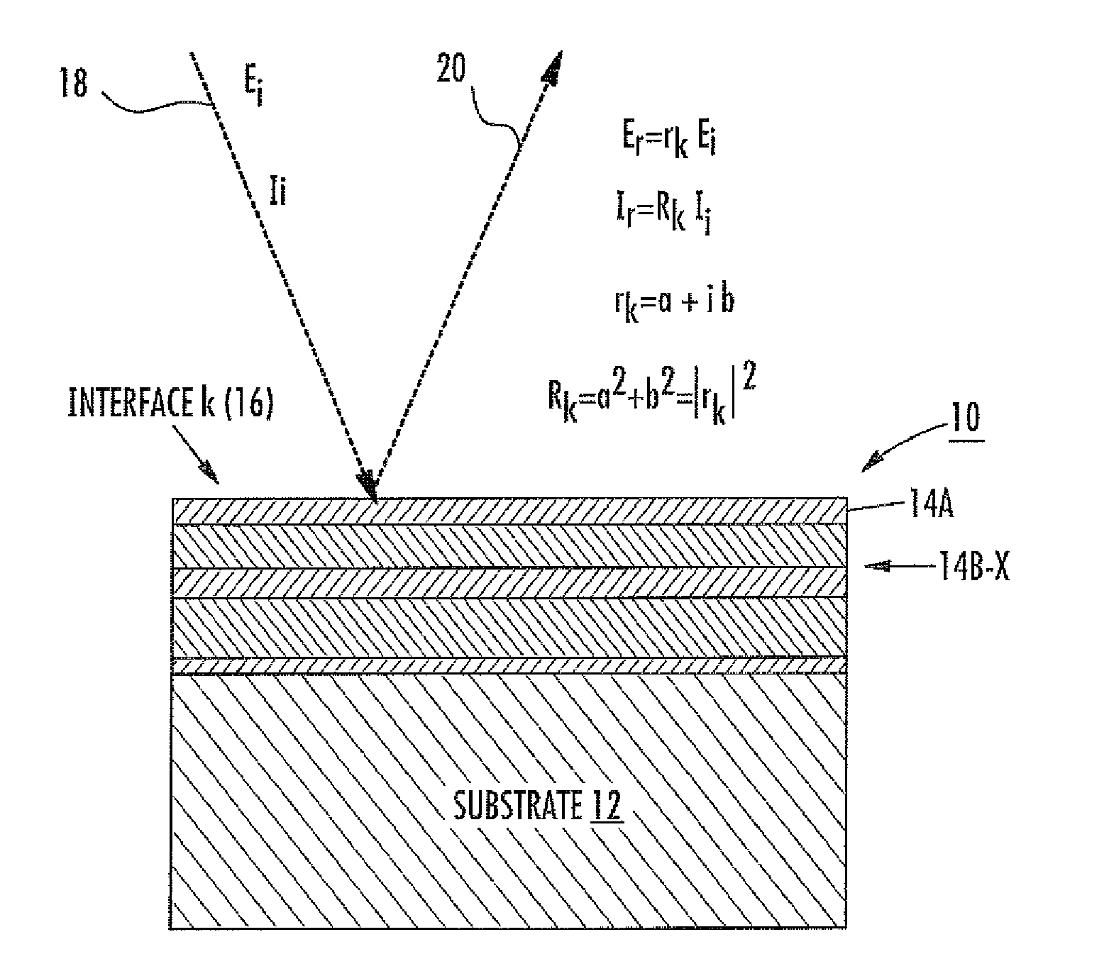
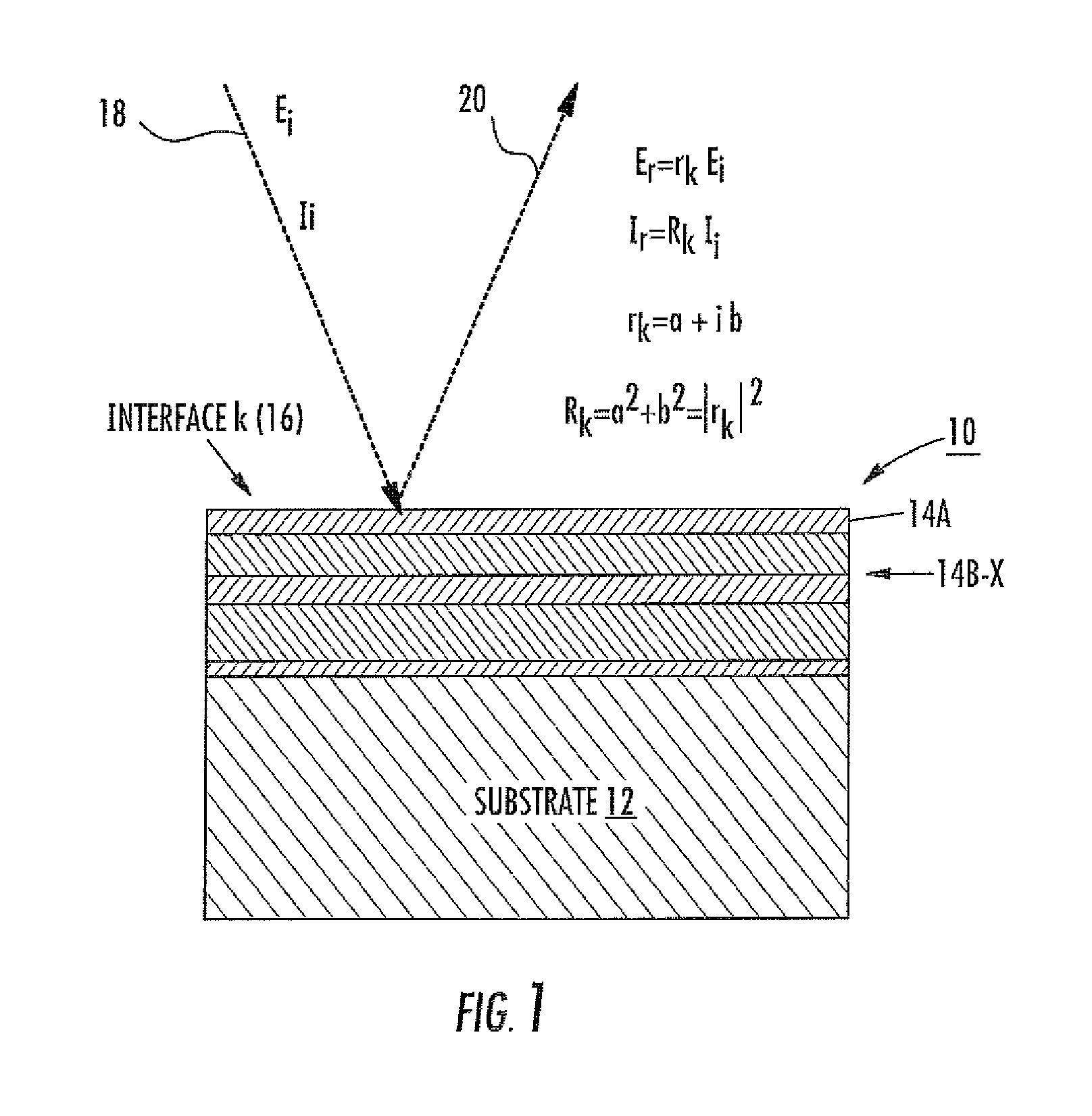
[0044]Turning now to the figures, FIG. 1 shows a thin film interference filter 10, wh...


PUM


Abstract

A thin film interference filter system includes a plurality of stacked films having a determined reflectance; a model monitor curve; and a topmost layer configured to exhibit a wavelength corresponding to one of the determined reflectance or the modeled monitor curve. The topmost layer is placed on the plurality of stacked films and can he a low-index film such as silica or a high index film such as niobia.

Description

CROSS-REFERENCE TO RELATED APPLICATIONS[0001]This application claims benefit of U.S. Provisional Patent Application, Ser. No. 60 / 609,406, entitled “Bootstrap Method for Interference Filter Thin Film Deposition Process Control,” filed Sep. 13, 2004.STATEMENT OF FEDERALLY SPONSORED RESEARCH OR DEVELOPMENT[0002]Research described in this application was sponsored by the United States Air Force Research Laboratory grant number F22615-00-2-6059.FIELD OF THE INVENTION[0003]The present invention relates to thin film optical devices. More particularly, the invention relates to complex interference filters.BACKGROUND OF THE INVENTION[0004]Highly accurate optical interference filters can be manufactured using thin film deposition processes. These optical interference filters are used for multivariate optical computing, multiple-band-pass, and the like and can exhibit complex optical spectra defined over a range of wavelengths. These filters are typically constructed by depositing alternating ...

Claims


Application Information

Patent Timeline
Patent Type & Authority Applications(United States)
IPC IPC(8): G06F17/11G06F17/10
CPCG01N21/55G02B5/28G01N2021/8438G01N21/8422
Inventor MYRICK, MICHAEL L.
Owner HALLIBURTON ENERGY SERVICES INC
Why Eureka
Try Eureka