Semiconductor device and abnormality detecting method

a technology of electromagnetic field and magnetic field, applied in the field of electromagnetic field, can solve the problem of not being able to execute secure abnormality detections with digital processing devices, and achieve the effect of secure detection of processing tasks

Inactive Publication Date: 2010-12-02
RENESAS ELECTRONICS CORP
View PDF6 Cites 50 Cited by
  • Summary
  • Abstract
  • Description
  • Claims
  • Application Information

AI Technical Summary

Benefits of technology

[0015]The semiconductor device of the present invention can securely detect the abnormality of the processing tasks executed by the software without imposing load on the CPU.

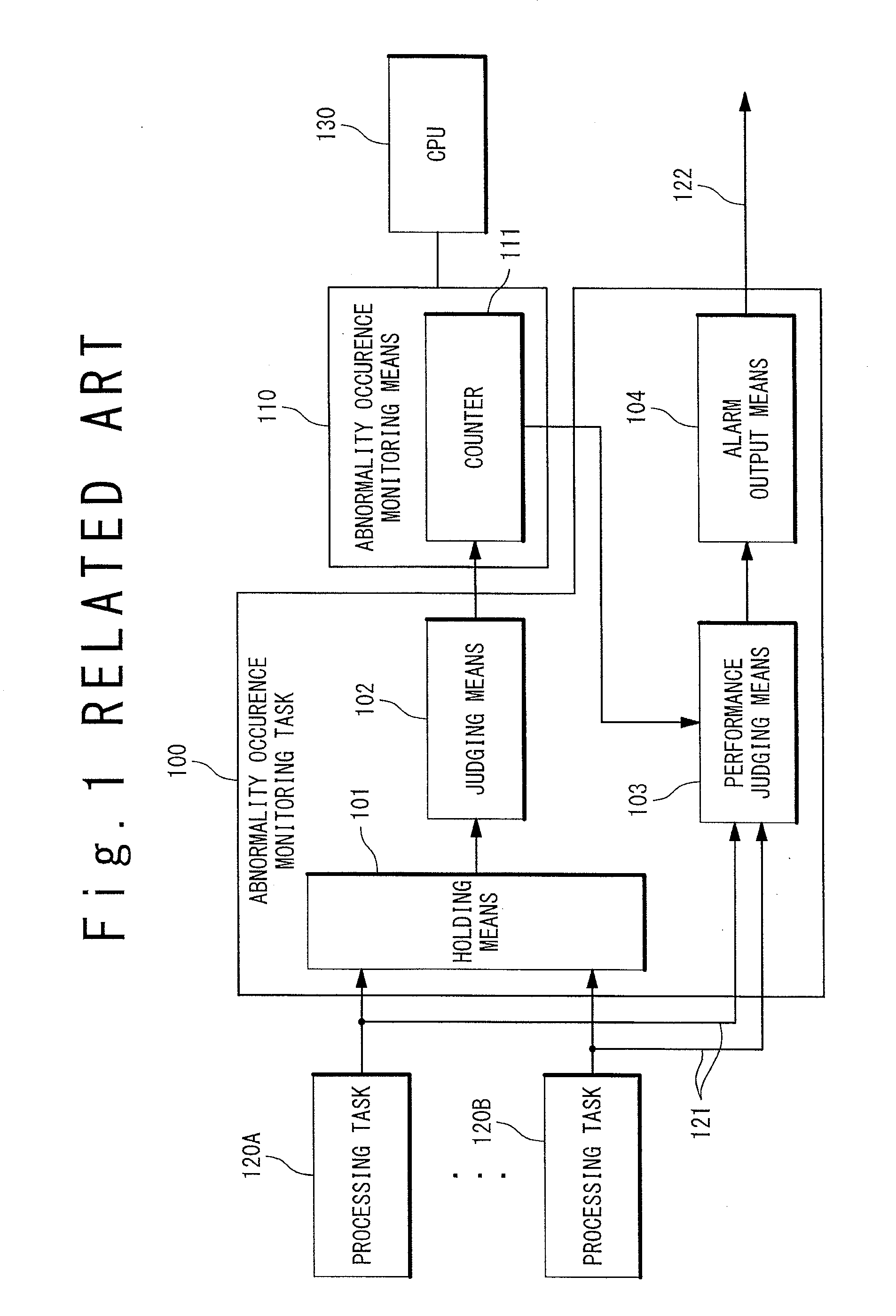
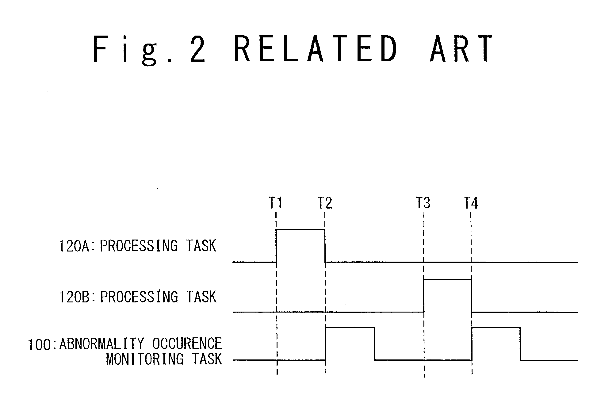
Problems solved by technology

However, as a result of conducting eager investigations, the inventors of the present invention have found that it is not possible to execute secure abnormality detections with the digital processing device of Patent Literature 1.

Method used


Image

  • Semiconductor device and abnormality detecting method
  • Semiconductor device and abnormality detecting method
  • Semiconductor device and abnormality detecting method

Examples


first embodiment

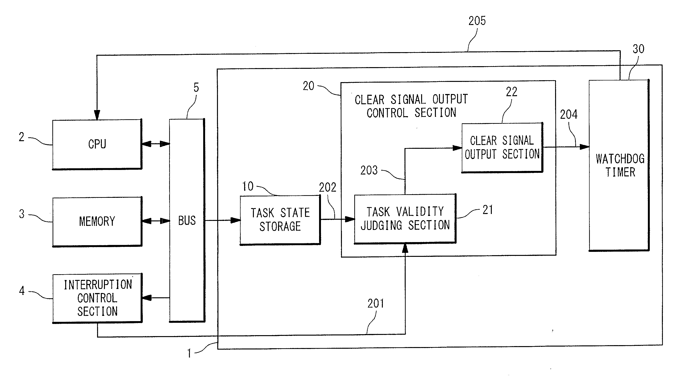
[0030]A semiconductor device and an abnormality detecting method will be described according to a first embodiment of the present invention. FIG. 4 is a block diagram showing an example of a configuration of an abnormality detecting section 1 that is a semiconductor integrated device according to the first embodiment of the present invention. Referring to FIG. 4, the abnormality detecting section 1 is connected to a bus 5, and a CPU (Central Processing Unit) 2, a memory 3, and an interruption control section 4 are connected to the bus 5. An input section for acquiring inputs of a user and an output section for having the user recognize a processing result may further be connected to the bus 5.

[0031]The CPU 2 executes software related to the present invention stored in the memory 3 to perform computing processing and control processing. The memory 3 is formed with a hard disk, a RAM (Random Access Memory), a ROM (Read Only Memory), or the like, which stores programs that implement ea...

second embodiment

[0110]A semiconductor device and an abnormality detecting method will be described according to a second embodiment of the present invention. FIG. 11 is a block diagram showing an example of the structure of an abnormality detecting section 1 that is a semiconductor integrated device according to the second embodiment of the present invention. In the second embodiment of the present invention, the abnormality detecting section 1 includes an output permission control section 40 in addition to the configuration of the first embodiment. The abnormality detecting section 1 according to the second embodiment of the present invention is different from that of the first embodiment in respect that the clear signal output section 22 is capable of executing operations based on a clear permission signal 206 outputted from the output permission control section 40 by ignoring the valid signal 203 outputted from the task validity judging section 21. Other configurational components are the same a...

third embodiment

[0118]A semiconductor device and an abnormality detecting method will be described according to a third embodiment of the present invention. FIG. 12 is a block diagram showing an example of a configuration of the abnormality detecting section 1 that is a semiconductor integrated device according to the third embodiment of the present invention. In the third embodiment of the present invention, the abnormality detecting section 1 further includes a DMA (Direct Memory Access) control section 50 which is connected to the CPU 2 and the memory 3 via the bus 5. Other configurational components are the same as those of the second embodiment, so that explanations thereof are omitted by simply applying same reference numerals to the same configurational components.

[0119]The DMA control section 50 generates an address of the execution state of the processing task existing in the memory 3 based on a startup request provided from the CPU 2 or based on the interruption signal 201. Further, the D...


PUM


Abstract

A semiconductor device comprises: a task state storage configured to store an executing state of a processing task of software executed by a CPU and to output an executing state signal to show the executing state of the processing task; a task validity judging section configured to acquire an interruption signal corresponding to the processing task based on a control of the CPU and the execution state signal, and to output a valid signal when the processing task is executed validly; a clear signal output section configured to output a clear signal in response to the valid signal; and a watchdog timer configured to clear a timer count value when the clear signal is acquired within a prescribed time and to output a reset signal when the clear signal is not acquired within the prescribed time.

Description

INCORPORATION BY REFERENCE [0001]This application claims the benefit of priority based on Japanese Patent Application No. 2009-128787, filed on May 28, 2009, the disclosure of which is incorporated herein by reference.BACKGROUND OF THE INVENTION[0002]1. Field of the Invention[0003]The present invention relates to a semiconductor device and, more specifically, to a method of detection of abnormality in software.[0004]2. Description of Related Art[0005]Semiconductor integrated circuits have become large-scaled year by year and functions to be mounted thereon have become complicated. Thus, the semiconductor integrated circuits have come to use software such as a real-time OS (Operating System) to achieve efficient controls. However, with the semiconductor integrated circuits using the real-time OS, there are increased cases of having a continuous high-load state in which the real-time OS simultaneously controls the functions, which may cause unexpectable abnormality. Therefore, it is r...

Claims


Application Information

Patent Timeline
Patent Type & Authority Applications(United States)
IPC IPC(8): G06F11/07
CPCG06F11/0757
Inventor KAMIYA, MAMORUHAZAKA, YOSHINORI
Owner RENESAS ELECTRONICS CORP
Why Eureka
Try Eureka