Device for detecting the thinning down of the substrate of an integrated circuit chip

a technology of integrated circuit chips and detection devices, which is applied in the direction of electrical/magnetic measurement arrangements, instruments, and using electrical/magnetic means, etc., can solve the problems of increasing the response time of the chip, and affecting the detection effect of integrity tests

Active Publication Date: 2010-12-16
STMICROELECTRONICS (ROUSSET) SAS
View PDF16 Cites 25 Cited by
  • Summary
  • Abstract
  • Description
  • Claims
  • Application Information

AI Technical Summary

Benefits of technology

[0012]Thus, an object of an embodiment of the present invention is to provide a device for detecting a laser attack, which overcomes at least some of the disadvantages of prior art solutions.
[0013]An object of an embodiment of the present invention is to provide a device enabling to detect the attack before the attacker is able to analyze the chip response to laser disturbances.
[0015]An object of an embodiment of the present invention is to provide a low-cost solution, easy to implement with usual manufacturing methods.

Problems solved by technology

Such devices may be subject to fraudulent manipulations aiming at obtaining protected confidential data.
Such solutions have the disadvantage of introducing additional calculation steps, thus increasing the chip response times. Further, integrity tests cannot detect all the disturbances caused by an attacker.
Like logic solutions, such solutions are not perfectly reliable.
Further, such solutions are expensive and difficult to implement.

Method used


Image

  • Device for detecting the thinning down of the substrate of an integrated circuit chip
  • Device for detecting the thinning down of the substrate of an integrated circuit chip
  • Device for detecting the thinning down of the substrate of an integrated circuit chip

Examples


Embodiment Construction

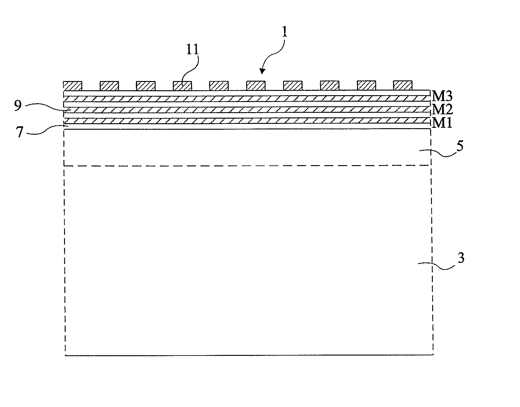
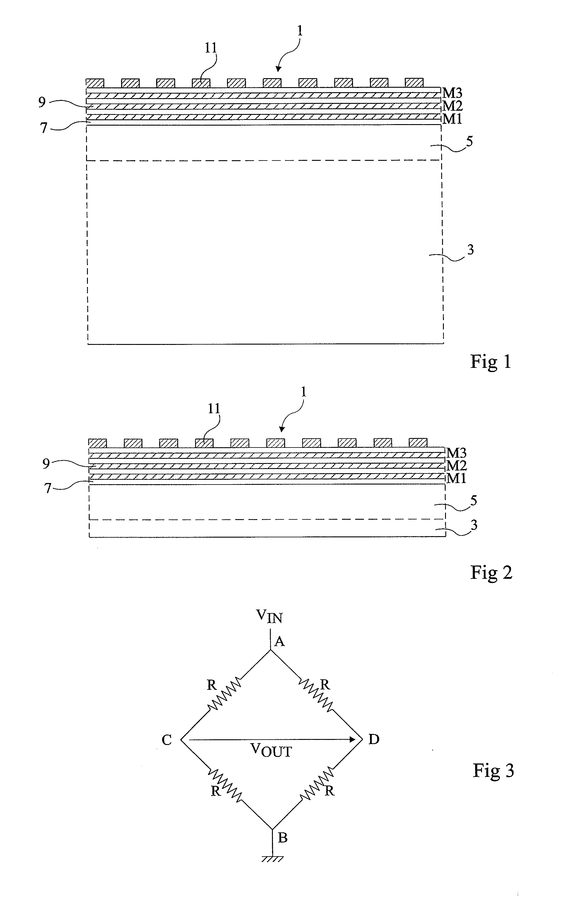
[0033]For clarity, the same elements have been designated with the same reference numerals in the different drawings and, further, as usual in the representation of integrated circuits, the various cross-section and top views are not drawn to scale.

[0034]FIG. 3 shows the electric diagram of a Wheatstone bridge formed of four resistors, for example, of same value R. A first voltage VIN is applied to a first diagonal of the bridge, between nodes A and B. An imbalance voltage VOUT may appear across a second diagonal of the bridge, between nodes C and D.

[0035]Normally, the Wheatstone bridge is balanced and output voltage VOUT is independent from the value of VIN and from possible temperature variations, for example, close to 0 V.

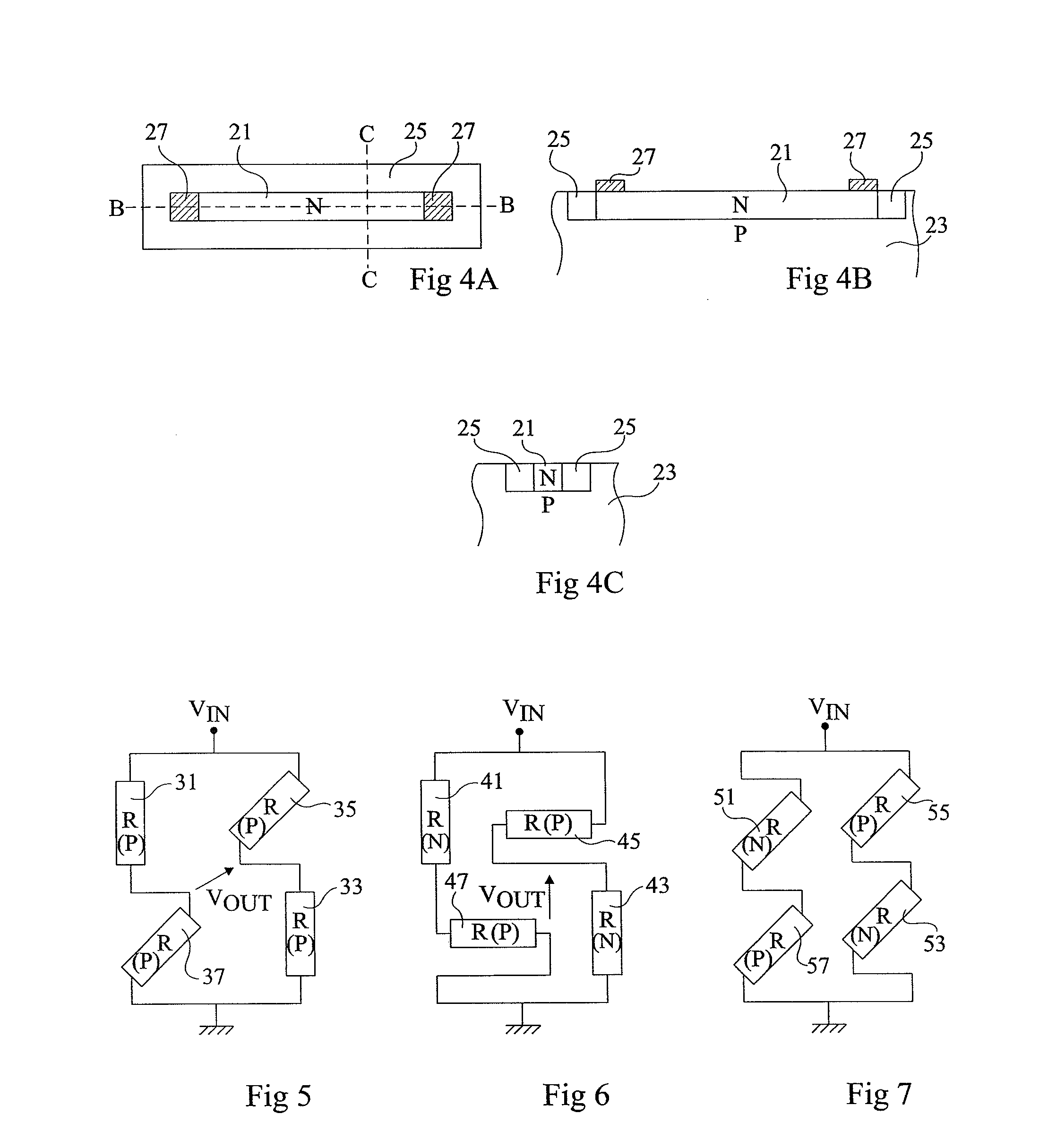
[0036]FIG. 4A is a top view schematically showing an embodiment of a diffused resistor. FIGS. 4B and 4C are cross-section views of FIG. 4A along axes B-B and C-C. An N-type doped area 21 is formed in the upper portion of a region 23 of a lightly-doped P-type sem...


PUM


Abstract

A device for detecting the thinning down of the substrate of an integrated circuit chip, including, in the active area of the substrate, bar-shaped diffused resistors connected as a Wheatstone bridge, wherein: first opposite resistors of the bridge are oriented along a first direction; the second opposite resistors of the bridge are oriented along a second direction; and the first and second directions are such that a thinning down of the substrate causes a variation of the imbalance value of the bridge.

Description

CROSS REFERENCE TO RELATED APPLICATIONS[0001]This application claims the priority benefit of French patent application number 09 / 53968, filed on Jun. 15, 2009, entitled “DEVICE FOR DETECTING THE THINNING DOWN OF THE SUBSTRATE OF AN INTEGRATED CIRCUIT CHIP,” which is hereby incorporated by reference to the maximum extent allowable by law.BACKGROUND OF THE INVENTION[0002]1. Field of the Invention[0003]The present invention relates to the protection of an integrated circuit chip against laser attacks. It more specifically aims at the detection of the thinning down of the chip substrate which is carried out before performing a laser attack.[0004]2. Discussion of the Related Art[0005]FIG. 1 is a simplified cross-section view of an integrated circuit chip 1 comprising a semiconductor support substrate 3, comprising in its upper portion an active layer 5 in which are formed electronic components, not shown. Substrate 3 is currently covered with a stack of insulating layers 7. Conductive in...

Claims


Application Information

Patent Timeline
Patent Type & Authority Applications(United States)
IPC IPC(8): G01R27/08
CPCG01L9/0042G06K19/07363G06K19/07381H01L22/34H01L23/576H01L2924/0002H01L2924/00G01R31/2851
Inventor FORNARA, PASCALRIVERO, CHRISTIAN
Owner STMICROELECTRONICS (ROUSSET) SAS
Why Eureka
Try Eureka