Nonvolatile semiconductor memory device and method for manufacturing same

a semiconductor memory and non-volatile technology, applied in semiconductor devices, semiconductor/solid-state device details, electrical devices, etc., can solve the problems of increasing the difficulty of achieving the effect of achieving the effect of achieving the effect of achieving the effect of achieving the effect of achieving the effect of achieving the effect of achieving the effect of achieving the effect of achieving the effect of achieving the effect of achieving the effect of achieving the effect of achieving the effect of achieving the effect o

Inactive Publication Date: 2010-12-23
KK TOSHIBA
View PDF7 Cites 255 Cited by
  • Summary
  • Abstract
  • Description
  • Claims
  • Application Information

AI Technical Summary

Problems solved by technology

The downscaling thereof has progressed acceleratingly, and limitations of downscaling are being approached.
While downscaling must be relied upon to increase the capacities of conventional structures having memory cells, circuit elements, and the like disposed in a plane, such downscaling has reached limitations.
In particular, the contact between transistors and interconnect layers included in the peripheral circuit easily deteriorate at high temperatures.

Method used


Image

  • Nonvolatile semiconductor memory device and method for manufacturing same
  • Nonvolatile semiconductor memory device and method for manufacturing same
  • Nonvolatile semiconductor memory device and method for manufacturing same

Examples


first embodiment

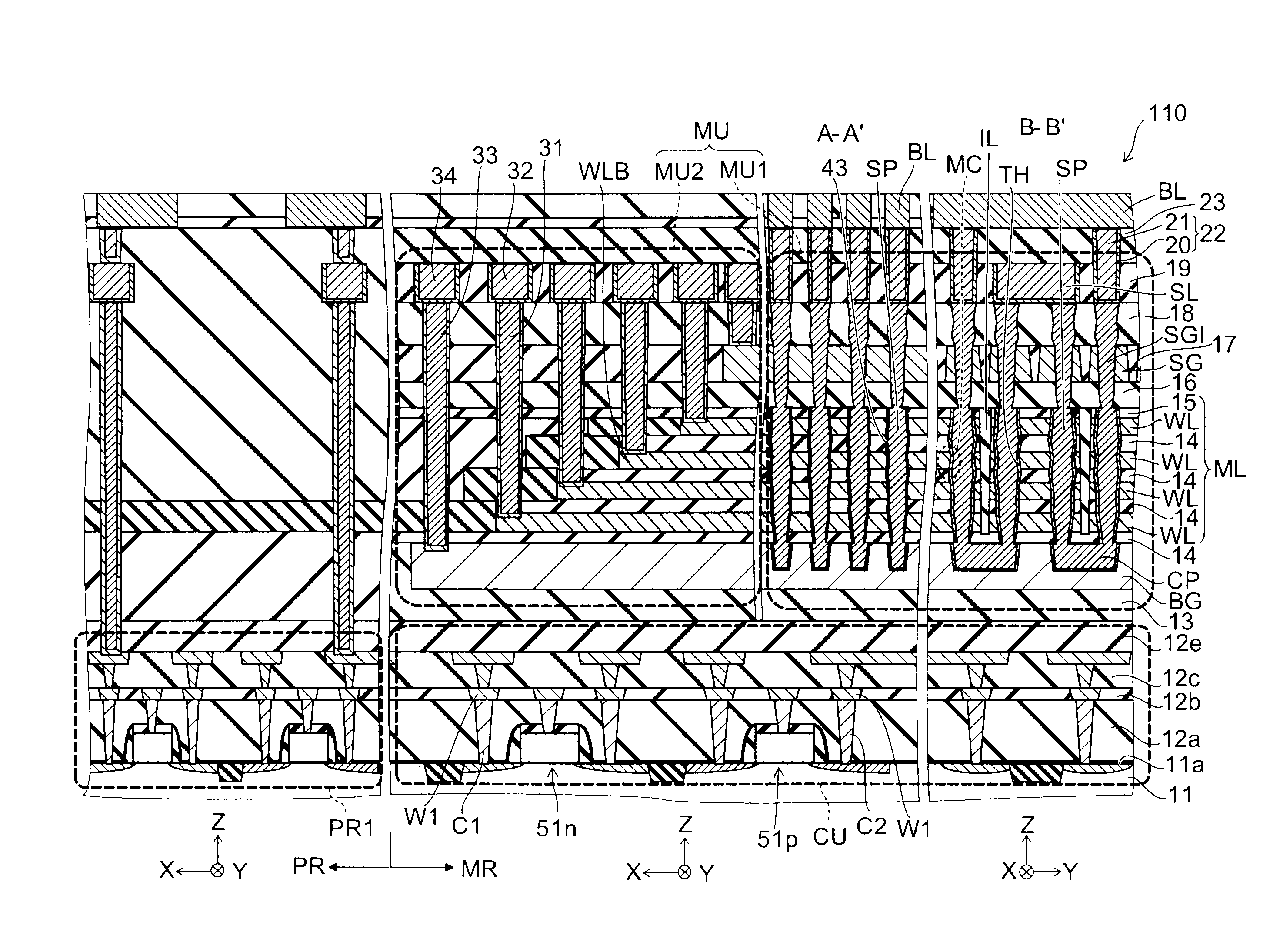
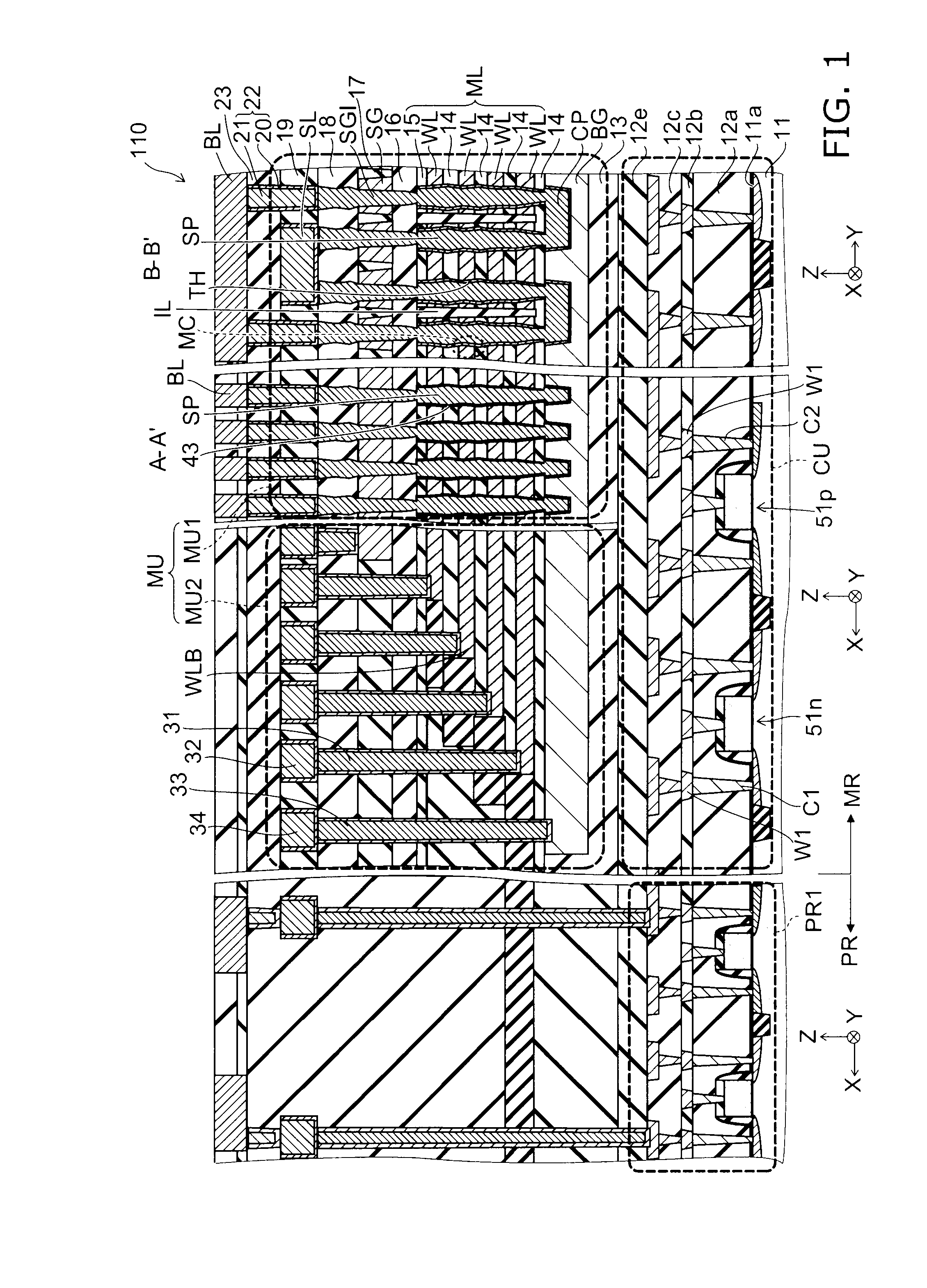
[0027]FIG. 1 is a schematic cross-sectional view illustrating the configuration of a nonvolatile semiconductor memory device according to a first embodiment of the invention.

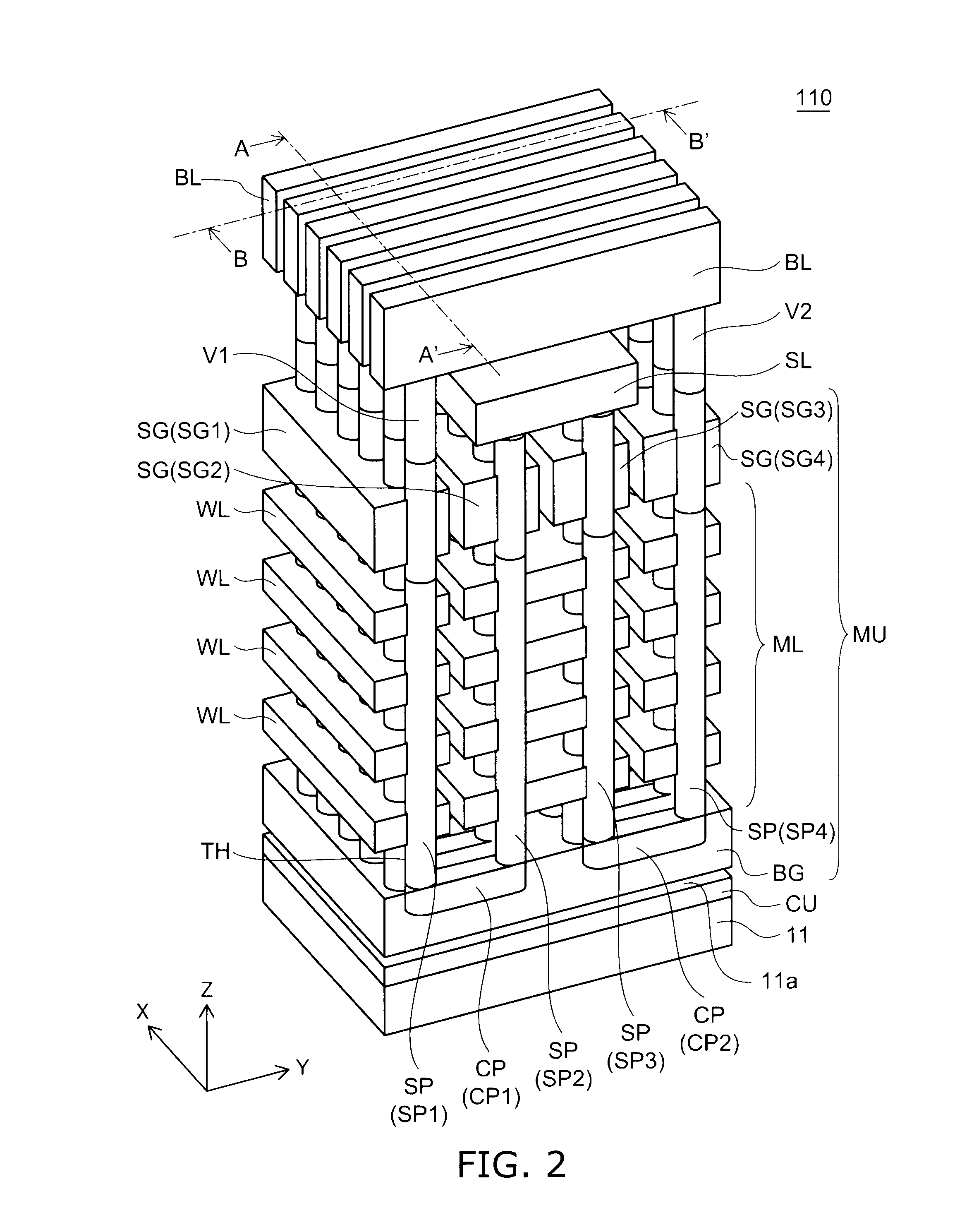
[0028]FIG. 2 is a schematic perspective view illustrating the configuration of the nonvolatile semiconductor memory device according to the first embodiment of the invention.

[0029]For easier viewing of the drawing in FIG. 2, only the conductive portions are illustrated, and the insulating portions are omitted.

[0030]A nonvolatile semiconductor memory device 110 according to the first embodiment of the invention is a three dimensional stacked flash memory.

[0031]As illustrated in FIG. 1, the nonvolatile semiconductor memory device 110 includes a semiconductor substrate 11 made of, for example, monocrystalline silicon.

[0032]A memory array region MR and a peripheral region PR are set in the semiconductor substrate 11 of this specific example. Memory cells are formed in the memory array region, and the peripheral regi...

second embodiment

[0146]FIG. 11 is a flowchart illustrating a method for manufacturing a nonvolatile semiconductor memory device according to a second embodiment of the invention.

[0147]FIGS. 12A and 12B are schematic cross-sectional views in order of the processes, illustrating the method for manufacturing the nonvolatile semiconductor memory device according to the second embodiment of the invention.

[0148]FIG. 13 is a schematic cross-sectional view in order of the processes, continuing from FIG. 12B.

[0149]In the method for manufacturing the nonvolatile semiconductor memory device according to this embodiment, first, the first transistor 51n and the second transistor 51p are formed on the major surface 11a of the semiconductor substrate 11, where the first transistor 51n includes the first source region 53n of the first conductivity type (e.g., the n-type) and the first drain region 54n of the first conductivity type, and the second transistor 51p includes the second source region 53p of the second c...


PUM


Abstract

A nonvolatile semiconductor memory device includes: a semiconductor substrate; a memory unit; and a circuit unit provided between the semiconductor substrate and the memory unit. The memory unit includes: a stacked structural unit having electrode films alternately stacked with inter-electrode-film insulating films; a semiconductor pillar piercing the stacked structural unit; and a storage unit provided corresponding to an intersection between the electrode films and the semiconductor pillar. The circuit unit includes first and second transistors having different conductivity type, a first interconnect, and first and second contact plugs. The first interconnect includes silicide provided on a side of the first and second transistors opposite to the semiconductor substrate. The first contact plug made of polysilicon of the first conductivity type connects the first interconnect to the first transistor. The second contact plug made of polysilicon of the second conductivity type connects the first interconnect to the second transistor.

Description

CROSS-REFERENCE TO RELATED APPLICATIONS[0001]This application is based upon and claims the benefit of priority from the prior Japanese Patent Application No. 2009-147605, filed on Jun. 22, 2009; the entire contents of which are incorporated herein by reference.BACKGROUND[0002]1. Field[0003]Embodiments of the invention relate generally to a nonvolatile semiconductor memory device for which electrical overwriting of data is possible and a method for manufacturing the same.[0004]2. Background Art[0005]Even higher capacities are desirable for nonvolatile semiconductor memory devices and particularly flash memory utilized in various applications. The downscaling thereof has progressed acceleratingly, and limitations of downscaling are being approached. While downscaling must be relied upon to increase the capacities of conventional structures having memory cells, circuit elements, and the like disposed in a plane, such downscaling has reached limitations.[0006]To solve such problems, fla...

Claims


Application Information

Patent Timeline
Patent Type & Authority Applications(United States)
IPC IPC(8): H01L29/792H01L21/336
CPCH01L23/522H01L23/53257H01L23/53271H01L27/11578H01L2924/0002H01L27/11582H01L2924/00H10B43/20H10B43/27H01L27/0688
Inventor KIDOH, MASARUKATSUMATA, RYOTAKITO, MASARUFUKUZUMI, YOSHIAKITANAKA, HIROYASUKOMORI, YOSUKEISHIDUKI, MEGUMIFUJIWARA, TOMOKOMIKAJIRI, YOSHIMASAOOTA, SHIGETOAOCHI, HIDEAKIKIRISAWA, RYOUHEIMATSUNAMI, JUNYA
Owner KK TOSHIBA
Why Eureka
Try Eureka