Method for the producing an electronic subassembly, as well as electronic subassembly

a technology of electronic subassembly and electronic subassembly, which is applied in the direction of printed circuit aspects, printed circuit non-printed electric components association, conductive pattern formation, etc., can solve the problems of difficult precise positioning of electronic components, difficult cutting of electronic components into circuit board substrates, and requiring complete removal of carrier foils. , to achieve the effect of high reliability, cost-effectiveness and cost-effectiveness

Inactive Publication Date: 2010-12-30
ROBERT BOSCH GMBH
View PDF7 Cites 15 Cited by
  • Summary
  • Abstract
  • Description
  • Claims
  • Application Information

AI Technical Summary

Benefits of technology

[0024]Furthermore, the method according to the present invention avoids risky mixed techniques in the production, such as soldering, adhesive bonding and wire bonding, for example. When the electronic subassembly is used in high-frequency technology, i.e., if the electronic component is a high-frequency component, then reproducible high-frequency transitions are achieved through the planar base structure obtained by the method according to the present invention.
[0025]Moreover, the method according to the present invention makes it possible to integrate possibly required heat sinks on power semiconductors. For instance, they may contact the electronic component on the side facing away from the conductive carrier foil. As an alternative, for example, it is also possible to embed them in the polymer mass by which the at least one electronic component is enclosed.
[0026]Furthermore, the method of the present invention makes it possible to achieve cost-effective wiring and encapsulation on many modules simultaneously.
[0027]In addition, the present invention relates to an electronic subassembly, which includes at least one electronic component connected to a circuit track structure on a circuit board, the at least one electronic component being embedded in the circuit board and the circuit track structure being situated at the surface of the circuit board. Apart from the cost-effective encapsulation already mentioned earlier and the resulting high reliability, the expensive substrate and packaging technology currently used in the related art is replaced or reduced to one small component. Moreover, with the electronic subassembly according to the present invention, a complete high-frequency circuit is able to be concentrated on one module, including antennas. The electronic subassembly produced according to the present invention is able to be processed further as a standard component.
[0028]In one example embodiment, the circuit track structure is implemented in a plurality of layers. This allows for better utilization of the surface of an electronic circuit board. Because of the additional layers the electronic subassembly is able to be fitted with components and contacted in a very confined space.
[0029]To provide excellent dissipation of the heat generated during the operation of the electronic subassembly, it is preferred if a metal core with a metal connection to the at least one electronic component is included in the circuit board.

Problems solved by technology

One disadvantage of this subassembly is that receptacles into which the electronic components are placed are cut into the circuit board substrate first.
This makes the precise positioning of the electronic components quite difficult.
One disadvantage of this method is that the carrier foil must be removed completely in order to obtain a functioning interconnection of the electric circuit.

Method used


Image

  • Method for the producing an electronic subassembly, as well as electronic subassembly
  • Method for the producing an electronic subassembly, as well as electronic subassembly
  • Method for the producing an electronic subassembly, as well as electronic subassembly

Examples


Embodiment Construction

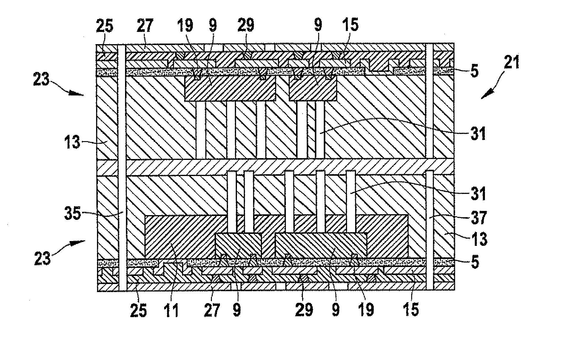
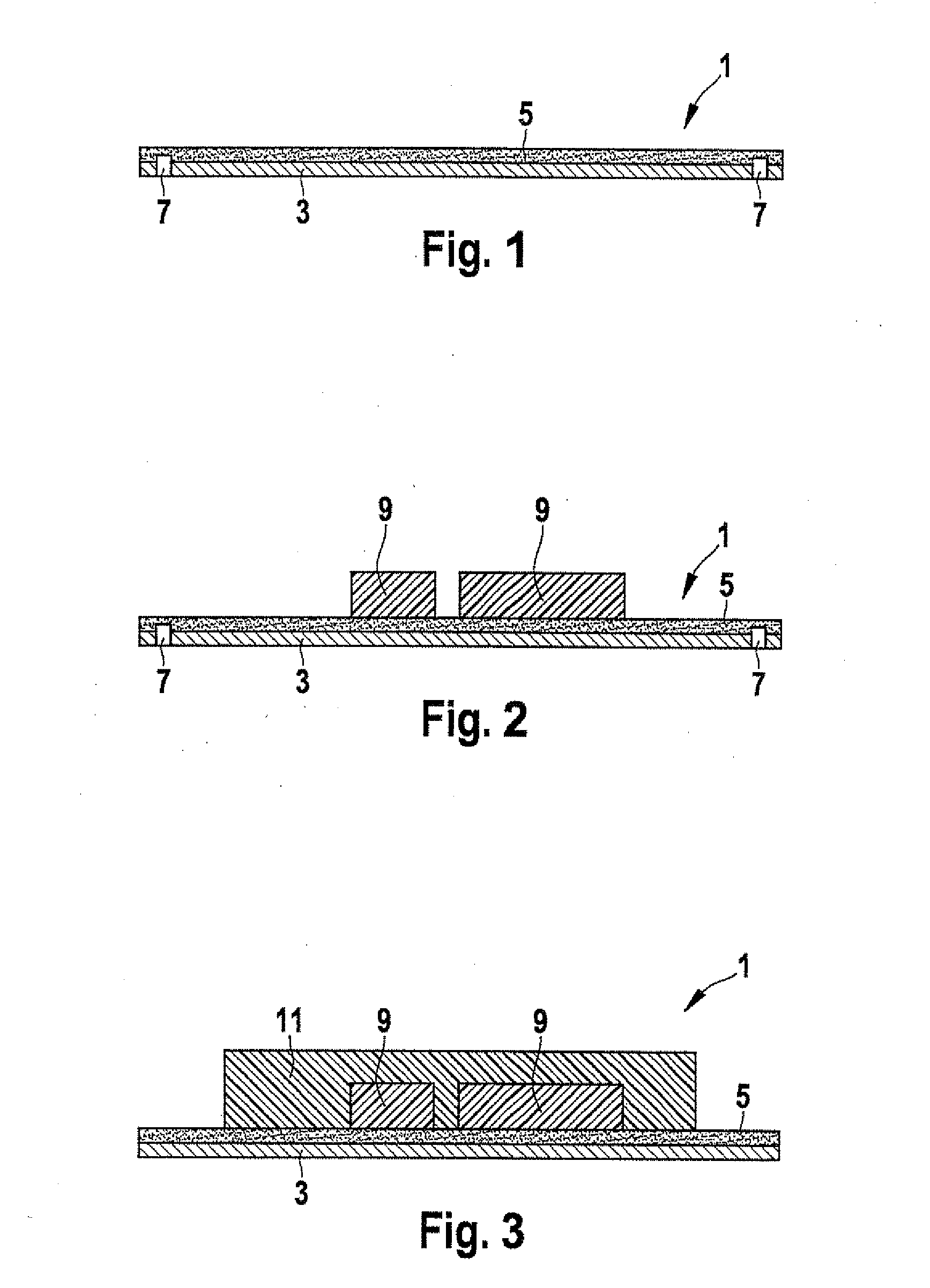
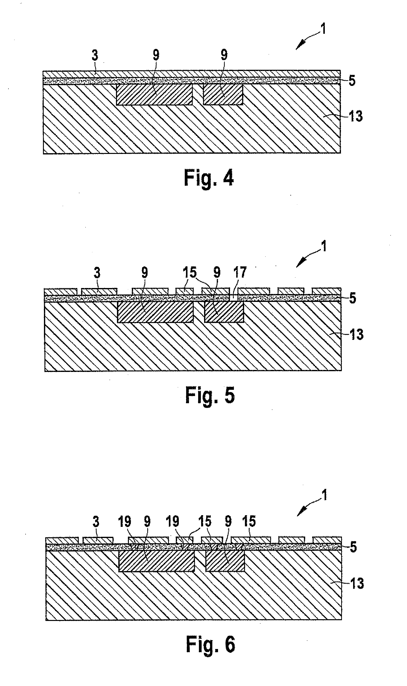
[0033]FIG. 1 shows a conductive carrier foil 1, which includes a conductive layer 3 and an insulating layer 5. Preferably, insulating layer 5 is an adhesive layer or a thermoplast on top of which electronic components are mountable. Alignment marks 7 are introduced on the side of conductive carrier foil 1 on which conductive layer 3 is located. For example, alignment marks 7 may be introduced into conductive carrier foil 1 by etching, stamping or drilling, e.g., laser drilling. Furthermore, it is also possible that the alignment marks are components connected to conductive carrier foil 1, which are exposed by drilling or detected by x-ray microscopy. Any other form of alignment marks known to one skilled in the art is possible as well.

[0034]Conductive layer 3 preferably is a metal layer. Especially preferred as metal is copper.

[0035]In a second step, electronic components 9 are mounted on insulating layer 5. This is illustrated in FIG. 2. In addition to electronic components 9, it i...


PUM

PropertyMeasurementUnit
thicknessaaaaaaaaaa
conductiveaaaaaaaaaa
massaaaaaaaaaa

Abstract

In a method for producing an electronic subassembly, at least one electronic component is mounted on an insulating layer of a conductive foil in a first step, the active side of the electronic component pointing in the direction of the conductive foil. In a second step, the conductive foil having the at least one electronic component mounted thereon is laminated to a circuit board substrate, the at least one electronic component pointing in the direction of the circuit board substrate. Finally, circuit tracks are developed by patterning the conductive foil, and the at least one electronic component is contacted.

Description

BACKGROUND OF THE INVENTION[0001]1. Field of the Invention[0002]The present invention relates to a method for producing an electronic subassembly including at least one electronic component, and also relates to an electronic subassembly including an electronic component.[0003]2. Description of Related Art[0004]To permit the encapsulation of electronic components used in electronic subassemblies on circuit boards and to increase the space utilization on the electronic circuit board, it is known to accommodate the electronic components within the circuit board. This protects the electronic components. From U.S. Pat. No. 6,512,182, for example, it is known to cut receptacles into a circuit board substrate, into which the electronic components are then placed. Once the electronic components have been inserted the receptacles are filled, then smoothed and laminated over. The embedding of the electronic components makes it possible to achieve a flat surface of the electronic subassembly.[...

Claims


Application Information

Patent Timeline
Patent Type & Authority Applications(United States)
IPC IPC(8): H05K1/18H05K3/30H05K3/10
CPCH01L24/18Y10T29/49146H01L2924/01013H01L2924/01029H05K1/0206H05K1/0207H05K1/0272H05K1/188H05K3/4602H05K3/4641H05K2201/0355H01L2924/01005H01L2924/01006H01L2924/01033H01L2924/1461H01L2224/18Y10T29/49155H01L2924/00H01L24/19H01L2224/04105H01L2924/19105
Inventor KUGLER, ANDREASBECKER, KARL-FRIEDERICHLIEBING, GERHARD
Owner ROBERT BOSCH GMBH
Why Eureka
Try Eureka