Digital heat injection by way of surface emitting semi-conductor devices

a semiconductor device and heat injection technology, applied in the field of digital heat injection by means of surface emitting semiconductor devices, can solve the problems of difficult generalization, slow change of shape in parts, sharp or abrupt change of shape in other parts, etc., and achieve the effect of improving the irradiation pattern

Active Publication Date: 2011-01-06
PRESSCO IP LLC
View PDF6 Cites 38 Cited by
  • Summary
  • Abstract
  • Description
  • Claims
  • Application Information

AI Technical Summary

Benefits of technology

[0021]In another aspect of the presently described embodiments, one of a lensing or reflector arrangement is superimposed between th...

Problems solved by technology

While each and every different material or compound has its own characteristic absorption curve shapes, they are often slow changing shapes in part of the curve and sharp or abruptly changing shapes in other portions of the curve.
Since every different type of material has its own characteristic curve shapes it is difficult to generalize, but while some materials will have gently changing absorption curves, many other materials will have areas of their absorption curve some place between UV and long infra-red which have rapidly or abruptly changing shapes.
The penalty for wavelength variation away from the desired center wavelength in such a case means that the irradiation would miss the peak and actually hit the target with energy that will be at a substantially different absorption than planned.
The result would require a large change in the amount of energy required to achieve the desired heating or energy deposition.
Typical diode or semi-conductor lasers however, have certain limitations and manufacturing challenges as well.
One troubling issue is the normal process variations that occur during manufacturing can cause the final laser devices to have a wider range of output wavelengths than is desired.
Of course, sometimes they can be used for another application that needs an adjacent wavelength, but this is not a reliable business plan for most situations.
This sorting procedure could easily cause the production yield to be below 20% when all the other production causes for fall-out are included.
This is a major problem for high-production, high-powered use of such devices.
The design of traditional diod...

Method used


Image

  • Digital heat injection by way of surface emitting semi-conductor devices
  • Digital heat injection by way of surface emitting semi-conductor devices
  • Digital heat injection by way of surface emitting semi-conductor devices

Examples


Embodiment Construction

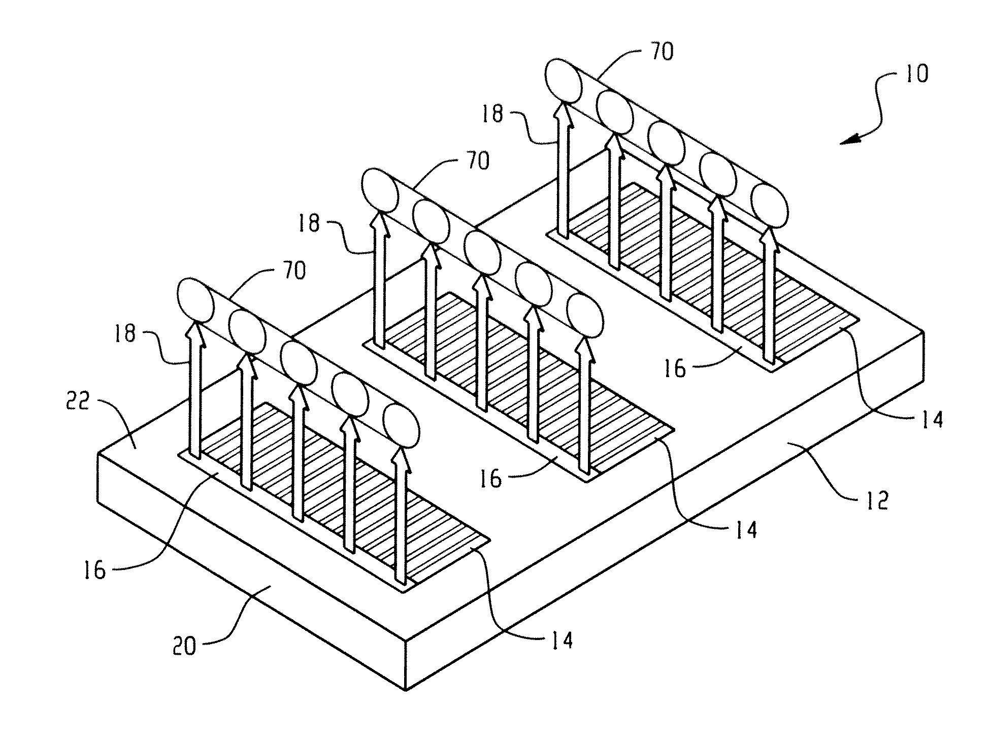
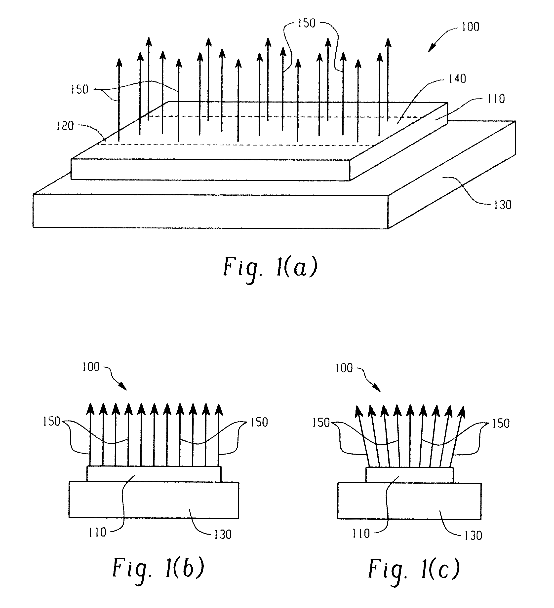
[0054]The present invention describes a new use of a documented but not well known laser diode technology. This is a new class of devices that are just emerging from a few advanced manufacturers as experimental devices and as a class are known as surface emitting diode lasers. They have unique properties for practicing digital heat injection technology and they have none of the limitations indicated above. Although they may not represent a substantial improvement for many traditional uses of laser diodes, they represent a substantially novel improvement in both the economics and the practicality of practicing digital heat injection technology.

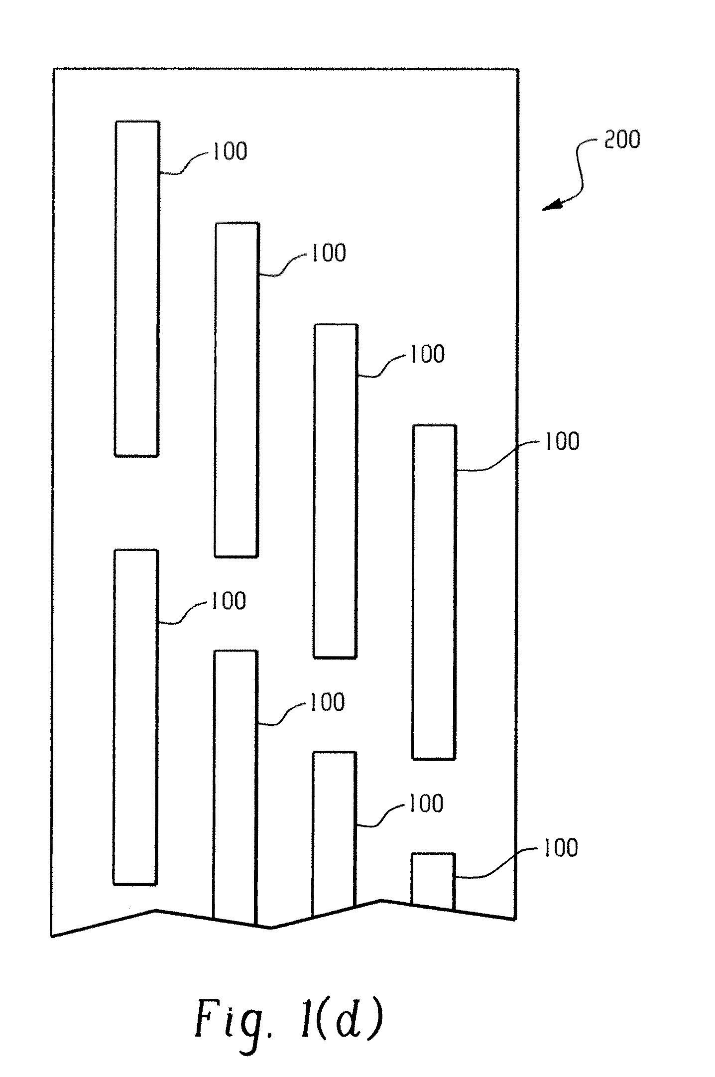
[0055]The design and manufacture of DHI applications typically involves a large number of laser diode devices for each system—since they are often involved in the radiating relatively large surface areas and heating target items with a substantial amount of energy. Many of the traditional applications for power laser diodes use small numbers of...


PUM

PropertyMeasurementUnit
Angleaaaaaaaaaa
Feed rateaaaaaaaaaa
Wavelengthaaaaaaaaaa

Abstract

A method and system are provided for digitally injecting heat into a wide range of products by way of incorporation of a special class of semi-conductor lasers, e.g. surface emitting devices. This technique relates to a more specific, economical, and advantageous way of practicing the art of directly injecting narrowband radiant energy that desirously matches the absorption specification of a particular material at a specified wavelength.

Description

[0001]This application is based on and claims priority to U.S. Provisional Application No. 61 / 224,765, filed Jul. 10, 2009, and U.S. Provisional Application No. 61 / 157,799, filed Mar. 5, 2009, both of which are incorporated herein by reference in their entirety.INCORPORATION BY REFERENCE[0002]U.S. Pat. No. 7,425,296; U.S. Ser. No. 11 / 448,630, filed Jun. 7, 2006; U.S. Ser. No. 12 / 135,739, filed Jun. 9, 2008 and U.S. Provisional Patent Application No. 61 / 157,799, filed Mar. 5, 2009, are hereby incorporated by reference in their entirety into the present disclosure.FIELD OF INVENTION[0003]This invention generally relates to a novel method of digitally injecting heat into a wide range of products by way of a novel incorporation of a special class of semi-conductor lasers, in one form, surface emitting devices. This invention relates to a more specific and advantageous way of practicing the art of directly injecting narrowband radiant energy that desirously matches the absorption specifi...

Claims


Application Information

Patent Timeline
IPC IPC(8): F26B3/28H01S5/18
CPCH01S5/423A47J37/00H01S5/0071H01S5/18H01S5/405B29C49/68A23L5/15H01S5/022H01S5/024H01S5/1203H05B3/0057H01S5/42H01S5/1082H01S5/02255
Inventor COCHRAN, DON W.JOHNSON, BENJAMIN D.KATZ, JONATHAN M.MOORE, MARK W.MORGAN, JR., NOEL E.ROSS, III, DENWOOD F.
Owner PRESSCO IP LLC
Why Eureka
Try Eureka