Graphene Device, Method of Investigating Graphene, and Method of Operating Graphene Device

a graphene device and graphene technology, applied in the field of graphene, can solve the problems of bandgap control, limited optical studies of bilayers, and inability to control,

Inactive Publication Date: 2011-01-13
RGT UNIV OF CALIFORNIA
View PDF8 Cites 57 Cited by
  • Summary
  • Abstract
  • Description
  • Claims
  • Application Information

AI Technical Summary

Problems solved by technology

However, in conventional materials, the bandgap is fixed by their crystalline structure, preventing such bandgap control.
Such control has proven elusive.
Optical studies of bilayers have so far

Method used


Image

  • Graphene Device, Method of Investigating Graphene, and Method of Operating Graphene Device
  • Graphene Device, Method of Investigating Graphene, and Method of Operating Graphene Device
  • Graphene Device, Method of Investigating Graphene, and Method of Operating Graphene Device

Examples


Embodiment Construction

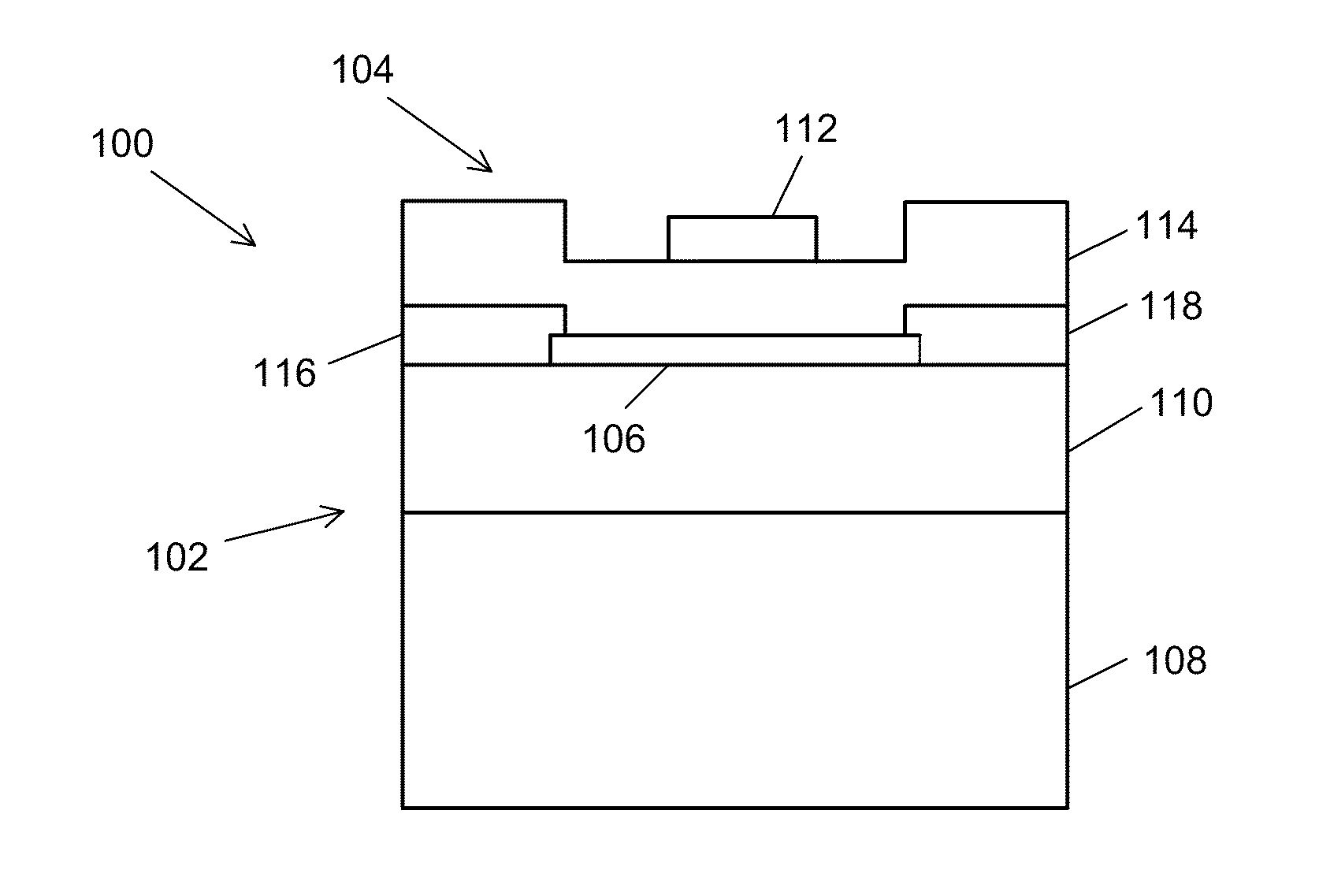
[0017]Embodiments of the present invention include a graphene device, a method of investigating semiconductor properties of bilayer graphene, and a method of operating a bilayer graphene device.

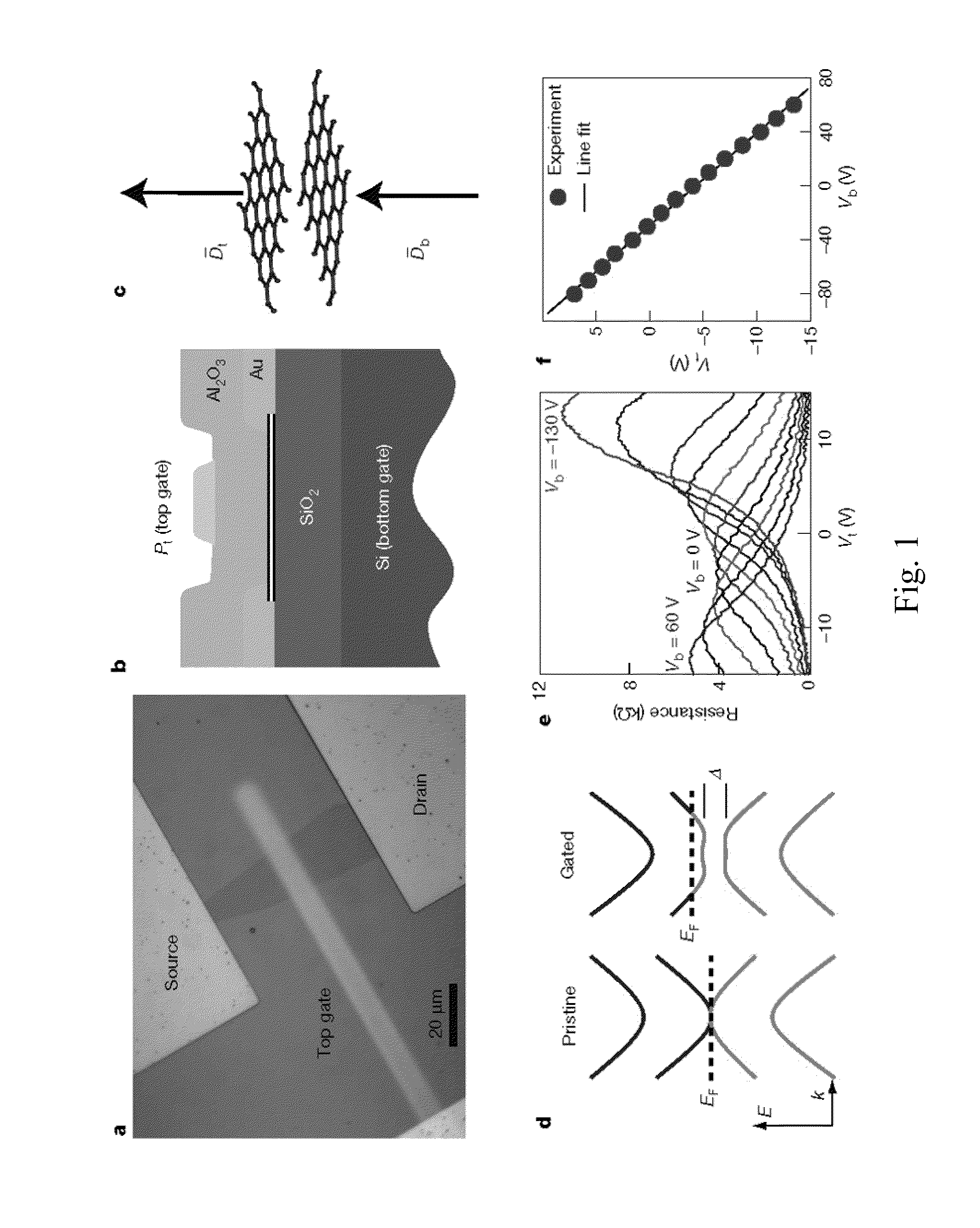
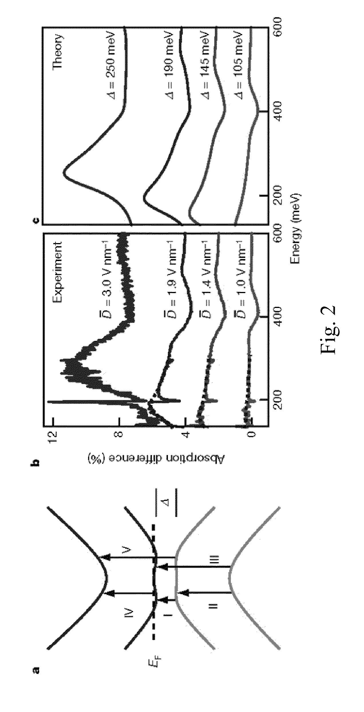
[0018]An embodiment of a bilayer graphene device of the present invention is illustrated in FIG. 6. The graphene device 100 includes a first gate structure 102, a second gate structure 104, and bilayer graphene 106. In an embodiment of the bilayer graphene device 100, the first gate structure 102 forms a substrate upon which the bilayer graphene device 100 is fabricated. The first gate structure 102 includes a first conducting layer 108 (i.e. a first gate) and a first insulating layer 110. For example, the first conducting layer 108 may be heavily doped silicon and the insulating layer 110 may be silicon dioxide. The second gate structure 104 is transparent or semi-transparent. For example, the second gate structure 104 may be transparent or semi-transparent within an infrared portion of the ...


PUM


Abstract

The present invention provides for a graphene device comprising: a first gate structure, a second gate structure that is transparent or semi-transparent, and a bilayer graphene coupled to the first and second gate structures, the bilayer graphene situated at least partially between the first and second gate structures. The present invention also provides for a method of investigating semiconductor properties of bilayer graphene and a method of operating the graphene device by producing a bandgap of at least 50 mV within the bilayer graphene by using the graphene device.

Description

RELATED APPLICATIONS[0001]The application claims priority to U.S. Provisional Patent Application Ser. No. 61 / 183,538, filed Jun. 2, 2009, which is herein incorporated by reference in its entirety.STATEMENT OF GOVERNMENT SUPPORT[0002]This invention was made with government support under Contract No. DE-AC02-05CH11231 awarded by the U.S. Department of Energy. The government has certain rights in this invention.BACKGROUND OF THE INVENTION[0003]The present invention relates to the field of graphene and, more particularly, to the field of graphene devices.[0004]The electronic bandgap is an intrinsic property of semiconductors and insulators that largely determines their transport and optical properties. As such, it has a central role in modern device physics and technology and governs the operation of semiconductor devices such as p-n junctions, transistors, photodiodes and lasers (ref. 1). A tunable bandgap would be highly desirable because it would allow great flexibility in design and...

Claims


Application Information

Patent Timeline
IPC IPC(8): G05F3/02H01L29/66G01N21/00
CPCH01L29/1606H01L29/7831H01L29/778H01L29/78684H01L29/78648
Inventor WANG, FENGZHANG, YUANBOTANG, TSUNG-TACROMMIE, MICHAEL F.ZETTL, ALEXANDER K.GIRIT, CAGLAR
Owner RGT UNIV OF CALIFORNIA
Why Eureka
Try Eureka