Large single crystal double layer graphene and the preparation method thereof

A technology of single-layer graphene and double-layer graphene, applied in graphene, chemical instruments and methods, inorganic chemistry, etc., can solve the problems of low coverage, small area and poor quality of double-layer graphene, and achieve improved The effect of growth efficiency

Active Publication Date: 2017-01-18
RENMIN UNIVERSITY OF CHINA
View PDF4 Cites 8 Cited by
  • Summary
  • Abstract
  • Description
  • Claims
  • Application Information

AI Technical Summary

Problems solved by technology

[0003] The purpose of the present invention is to provide a large single-crystal double-layer graphene and its preparation method. The present invention provides a method for preparing large-area high-quality double-layer graphene with

Method used


Image

  • Large single crystal double layer graphene and the preparation method thereof
  • Large single crystal double layer graphene and the preparation method thereof
  • Large single crystal double layer graphene and the preparation method thereof

Examples


Embodiment 1

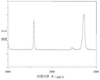
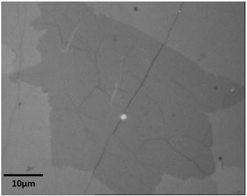
[0039] Embodiment 1, the bilayer graphene that is coated with the silicon substrate of 300nm silicon dioxide growth

[0040] Follow the steps below to grow bilayer graphene on a silicon substrate coated with 300nm silicon dioxide:

[0041] (1) Preparation of single-layer graphene and transfer

[0042] Using chemical vapor deposition equipment, based on the optimized growth conditions on the copper substrate, first obtain high-quality single-layer graphene, use wet transfer, first spin-coat PMMA glue on the single-layer graphene copper sheet, and bake the glue After 30 minutes, use ammonium persulfate to remove the copper sheet, pick up the film with a silicon substrate, and let it air-dry overnight. Then use acetone to remove the PMMA glue on the surface of the sample to obtain a single-layer graphene film transferred on the silicon substrate.

[0043] (2) Preparation of bilayer graphene by CVD system

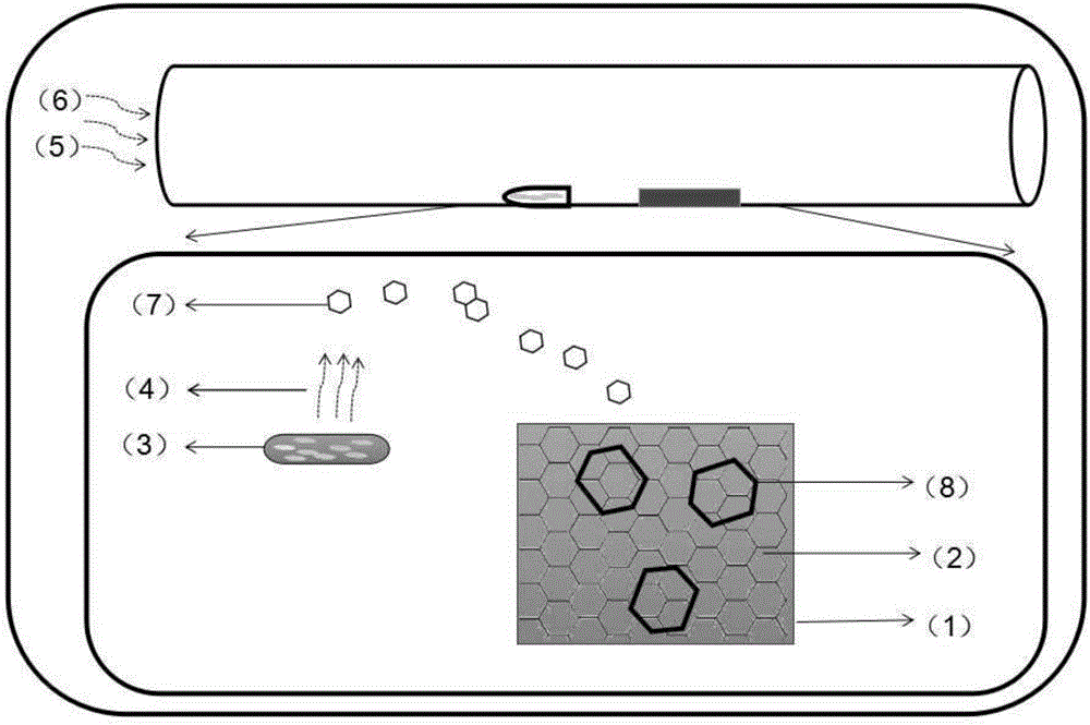
[0044] Such as figure 1As shown, the nano-copper powder is packed in a ...

Embodiment 2

[0049] Embodiment 2, double-layer graphene grown on sapphire substrate

[0050] Follow the steps below to grow bilayer graphene on a sapphire substrate:

[0051] (1) Preparation of single-layer graphene and transfer

[0052] Using chemical vapor deposition equipment, based on the optimized growth conditions on the copper substrate, first obtain high-quality single-layer graphene, the transfer method is the same as in Example 1, except that the sapphire substrate is used when the film is finally picked up, that is, the transfer on the sapphire is obtained. Single-layer graphene films on substrates.

[0053] (2) Preparation of bilayer graphene by CVD system

[0054] This step is identical with embodiment 1, and difference is: insulating substrate is sapphire substrate; The spacing between small quartz tube and sapphire substrate is 5cm; When growing double-layer graphene, the rate that feeds methane is 20sccm, The rate of introducing hydrogen gas is 100 sccm; the temperature ...


PUM


Abstract

The invention discloses a large single crystal double layer graphene and the preparation method thereof. The method comprises the steps of selecting a single layer graphene as the seed layer, applying the chemical vapor deposition to cultivate graphene on the edge liner to obtain the double layer graphene on the insulated liner. The invention applies the single layer graphene as the seed layer of the double layer graphene and controls the development of the extensive growth of the double graphene by the chemical vapor deposition, thus achieving the control of the pile structure of the double layer graphene. The use of copper powder of nano scale and other catalysts can steam out the copper particulates, which is transported to the reactor liner by the steam, the catalyst decomposes the carbon source to acquire the carbon atoms or carbon atom groups which floats to the liner of the full layer of the single layer graphene to cultivate the double layer graphene on the extension of the single layer graphene. The method enhances the cultivation efficiency and achieves the top-to-bottom-piling preparation.

Description

technical field [0001] The invention relates to a large single-crystal double-layer graphene and a preparation method thereof. Background technique [0002] Graphene has a unique bandgap structure and physical properties. Among them, single-layer graphene has a zero-bandgap structure, which has certain limitations in the application of semiconductor devices, but when the number of layers increases, the bandgap of graphene is opened. For example, the bandgap of bilayer graphene can be tuned up to 250 meV under an applied electric field. Mechanical exfoliation is commonly used to obtain bilayer graphene, but the area is only a few microns. In recent years, chemical vapor deposition has been widely used to prepare bilayer graphene, but so far, the coverage of bilayer graphene is not high and the uniformity is not good, and the stacking method between layers cannot be controlled very well. . However, the current method of multilayer graphene on an insulating substrate is sti...

Claims


Application Information

Patent Timeline
IPC IPC(8): C01B32/186
CPCC01B2204/04C01P2002/74C01P2002/82C01P2004/03C01P2004/04
Inventor 陈珊珊王伟伟陈香萍
Owner RENMIN UNIVERSITY OF CHINA
Why Eureka
Try Eureka