Memristor with two-dimensional material heterojunction and preparation method thereof

A two-dimensional material, heterojunction technology, applied in the field of microelectronics, can solve problems such as difficult to meet application requirements, no one has provided new memristors, etc., to reduce growth time and capital costs, ultra-thin thickness, and reduce manufacturing costs. Effect

Active Publication Date: 2019-11-29
HUAZHONG UNIV OF SCI & TECH
View PDF4 Cites 10 Cited by
  • Summary
  • Abstract
  • Description
  • Claims
  • Application Information

AI Technical Summary

Problems solved by technology

However, due to the limitations of the material itself in terms of mechanics and optics, it is difficult to meet the application requirements of flexibility and transparency in the future, and it also faces many challenges such as device structure size, stability and operating voltage.
At present, no one has provided a technical solution for the construction of new memristors based entirely on two-dimensional materials.

Method used


Image

  • Memristor with two-dimensional material heterojunction and preparation method thereof
  • Memristor with two-dimensional material heterojunction and preparation method thereof
  • Memristor with two-dimensional material heterojunction and preparation method thereof

Examples


Embodiment 1

[0044] In the following embodiments, different electrode materials and different intermediate dielectric layers (ie, different two-dimensional material heterojunction layers) are used to realize the preparation of novel memristor devices.

[0045] combine figure 2 Embodiment 1 is specifically introduced as follows:

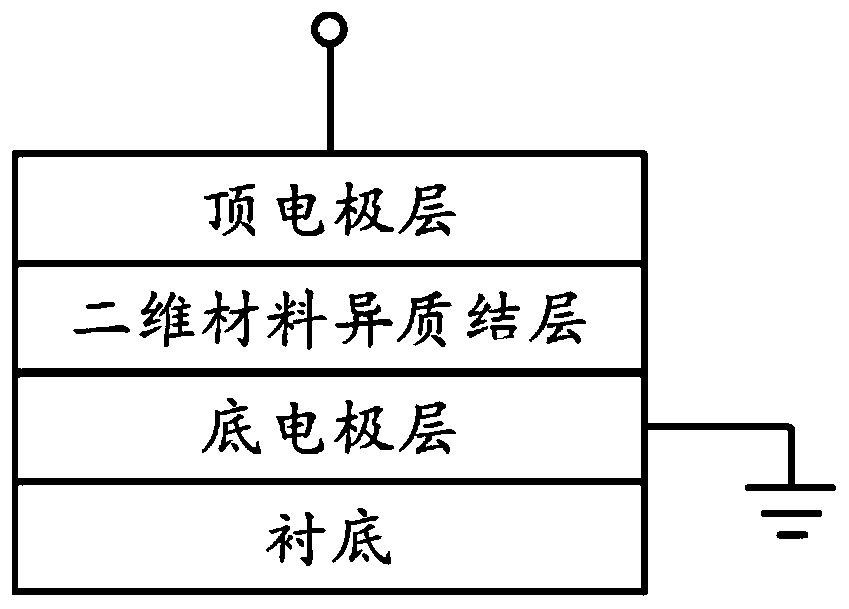
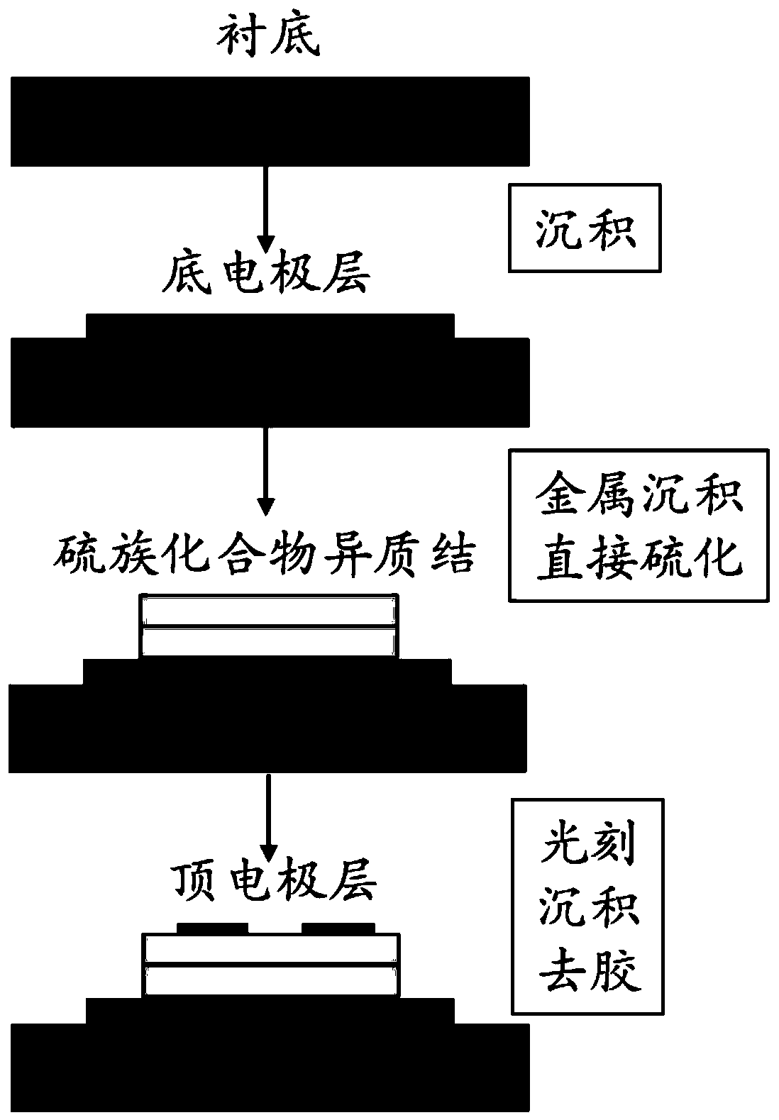
[0046] The two-dimensional material heterojunction memristor in Example 1 includes sequentially forming a bottom electrode layer and a memristive dielectric layer on the substrate, and forming a top electrode layer on the memristive dielectric layer, and the memristive dielectric layer is Two-dimensional material heterojunction. The bottom electrode layer of this embodiment 1 uses ITO conductive glass; the middle memristive dielectric layer is WS prepared by solid phase vulcanization method. 2 / MoS 2 The heterojunction has a thickness of 5nm; the top electrode layer is made of metal aluminum film with a thickness of 100nm.

[0047] The preparation method of t...

Embodiment 2

[0060] In this embodiment, except for the intermediate dielectric layer WS 2 / MoS 2 The thickness of the heterojunction is 20nm, and the thickness of the tungsten sulfide and the molybdenum sulfide are both 10nm. Other specific implementation methods are the same as the above-mentioned embodiment 1.

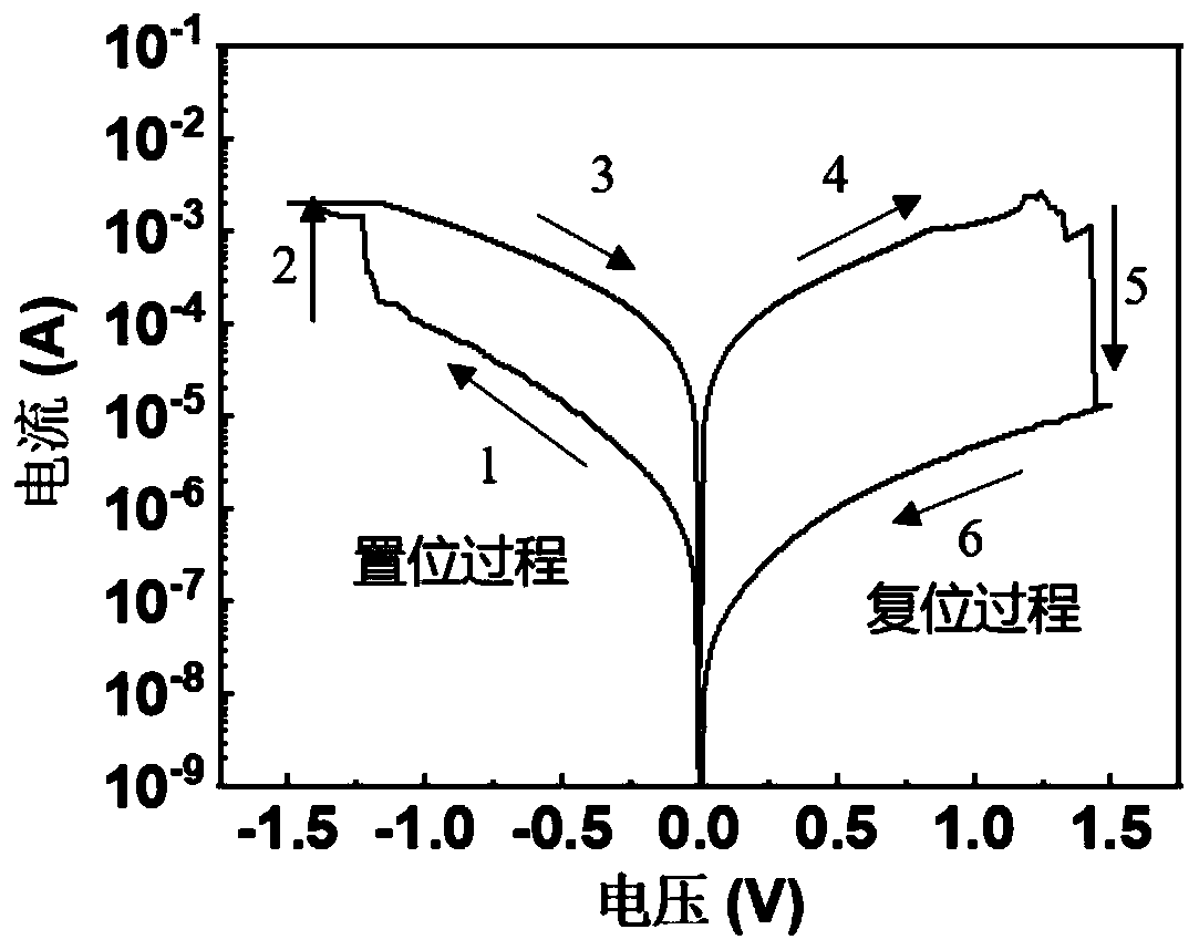
[0061] Further, in this embodiment, for the WS through the semiconductor parameter analyzer 2 / MoS 2Heterojunction memristors were tested electrically. Figure 7 Shown is the test chart of the current-voltage characteristic curve of the memristor in the initial state under the action of the DC sweep voltage of this embodiment.

Embodiment 3

[0063] In this embodiment, except that the top electrode layer is Ag with a thickness of 100 nm, other specific implementation methods are the same as the above embodiment 1.

[0064] Further, in this embodiment, for the WS through the semiconductor parameter analyzer 2 / MoS 2 Heterojunction memristors were tested electrically. Figure 8 Shown is the test chart of the current-voltage characteristic curve of the memristor in the initial state under the action of the DC sweep voltage of this embodiment.


PUM

PropertyMeasurementUnit
thicknessaaaaaaaaaa
thicknessaaaaaaaaaa
thicknessaaaaaaaaaa

Abstract

The invention belongs to the technical field of microelectronics, and discloses a memristor with a two-dimensional material heterojunction and a preparation method of the memristor. The memristor comprises a substrate, a bottom electrode layer, a two-dimensional material heterojunction layer and a top electrode layer from bottom to top, wherein the two-dimensional material heterojunction layer serves as an intermediate dielectric layer and is of a two-layer laminated structure composed of two different metal sulfur compounds, and each layer in the laminated structure corresponds to one metal sulfur compound. Compared with the prior art, the novel memristor is constructed completely based on a two-dimensional material by improving a key functional layer material adopted by the device, the overall structural design of the device and the like, the traditional MIM structure is overturned, and the memristor has the characteristics of low working voltage, fatigue resistance and cycling stability. In addition, the memristor shows high similarity with synapses in information transmission on the aspect of simulating information transmission of neuron, and has a great application prospect onthe development of brain-like structures in the future.

Description

technical field [0001] The invention belongs to the technical field of microelectronics, and more specifically relates to a memristor of a two-dimensional material heterojunction and a preparation method thereof. Background technique [0002] In 1971, Professor Cai Shaotang of the University of California, Berkeley boldly predicted from the perspective of physical symmetry that in addition to the known three basic circuit passive components of resistance, capacitance and inductance, there should be a fourth basic component "memristor": The resistance value of this element depends on the history of the input current or voltage, that is, it has memory characteristics. After 37 years, the engineers of Hewlett-Packard Labs announced in the "Nature" magazine that they had physically discovered the fourth basic circuit element for the first time, which immediately aroused great attention from the global electronics industry. [0003] Although the emergence of memristors has trigg...

Claims


Application Information

Patent Timeline
Patent Type & Authority Applications(China)
IPC IPC(8): H01L45/00
CPCH10N70/20H10N70/882H10N70/881H10N70/011H01L29/8615H01L29/66969H01L29/24H01L29/45H01L29/0665H01L21/02568H01L21/02485H01L21/02614H01L21/02425B82Y10/00H10N70/8822H10N70/826H10N70/021H01L21/0242H01L21/02491H01L29/242H01L29/86
Inventor 熊伟张文广邓磊敏刘敬伟吴昊段军
Owner HUAZHONG UNIV OF SCI & TECH
Why Eureka
Try Eureka