Graphene photoeletric modulator based on slot waveguide

An electro-optical modulator and slit waveguide technology, which is applied in the field of integrated optics and silicon-based photonics, can solve the problems affecting the modulation bandwidth of the modulator and limit the minimum size of graphene, so as to facilitate batch production and system integration, reduce Small size, enhance the effect of interaction

Active Publication Date: 2019-02-26
BEIJING UNIV OF POSTS & TELECOMM
View PDF3 Cites 9 Cited by
  • Summary
  • Abstract
  • Description
  • Claims
  • Application Information

AI Technical Summary

Problems solved by technology

In order to be able to transmit in the waveguide, the size of the silicon-based waveguide must meet the single-mode cut-off co

Method used


Image

  • Graphene photoeletric modulator based on slot waveguide
  • Graphene photoeletric modulator based on slot waveguide

Examples


Embodiment Construction

[0021] The present invention will be further described below in conjunction with the accompanying drawings.

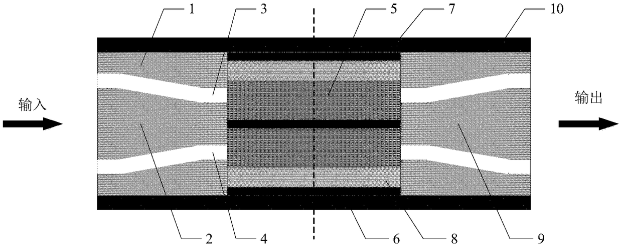
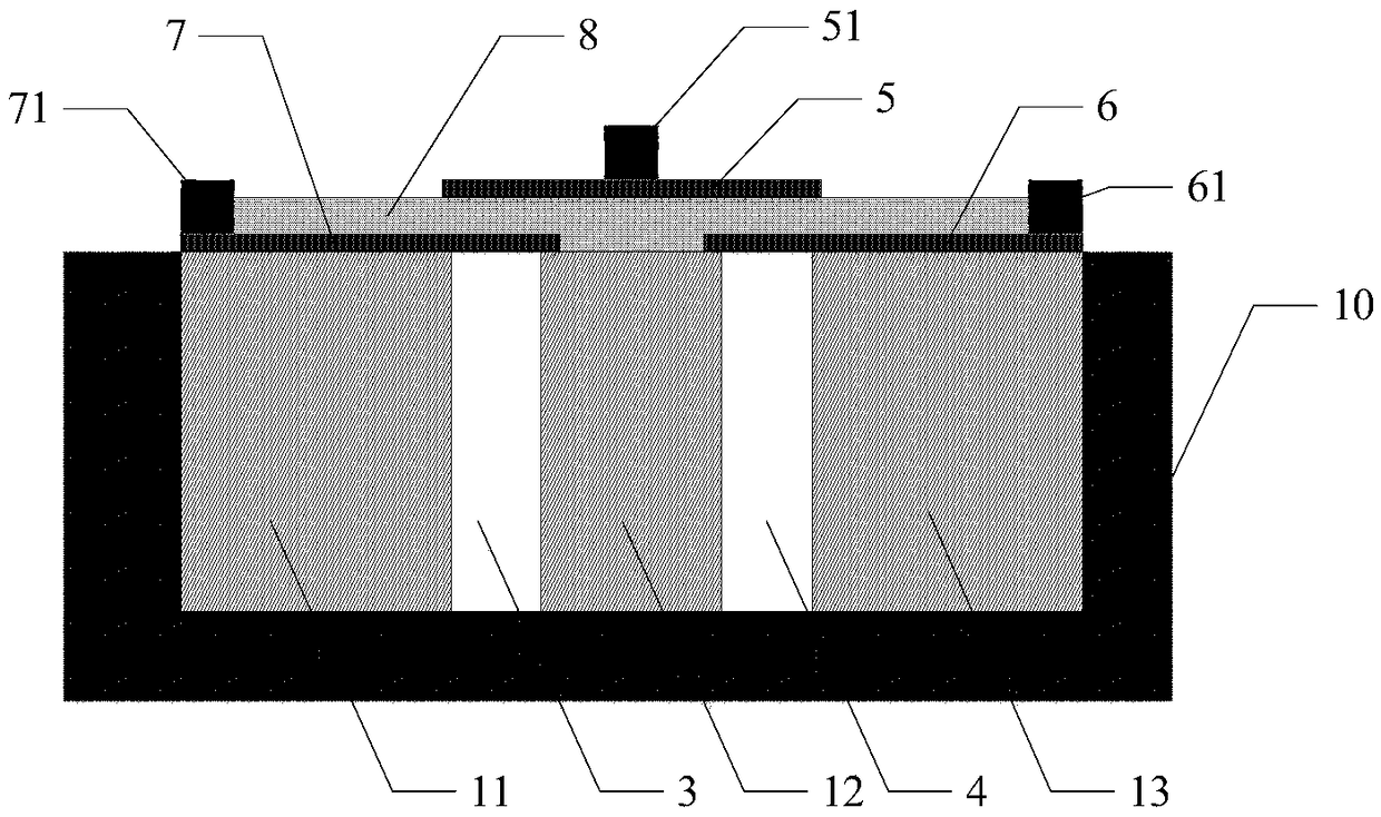
[0022] From figure 1 It can be seen that the graphene electro-optic modulator based on the slot waveguide of the present invention is a silicon-based waveguide Mach-Zehnder interference structure modulator fabricated on an SOI silicon wafer. devices include SiO 2 A substrate layer (10), a silicon optical waveguide (1), a dielectric filling layer (8) and an electrode structure. Among them, the silicon-based waveguide (1) is a buried waveguide structure; the optical signal first passes through the slit waveguide beam splitter (2) to couple the optical signal into the two arms of the Mach-Zehnder interference structure, the first slit waveguide (3) and the second The slit waveguide (4); by adjusting the graphene electrodes above the slit waveguide respectively, changing the refractive index of the slit waveguide to realize the modulation of the light field phase. The o...


PUM

PropertyMeasurementUnit
Thicknessaaaaaaaaaa

Abstract

The invention discloses a graphene photoelectric modulator based on a slot waveguide, which belongs to the field of integrated photons and silicon-based photonics. An optical modulator includes substrate layer, silicon optical waveguide, dielectric filling layer and electrode structure. The silicon optical waveguide structure is buried in the substrate layer, and the silicon optical waveguide is aMach-Zehnder interference structure composed by a silicon slot waveguide, including a slot waveguide splitter, a first slot waveguide, a second slot waveguide and a slot waveguide combiner. The firstslit waveguide consists of a first silicon waveguide and a second silicon waveguide; the second slot waveguide consists of a second silicon waveguide and a third silicon waveguide; a first graphene layer and a third graphene layer are covered on the first slot waveguide; a second graphene layer and a third graphene layer are covered on the second slot waveguide; the third graphene layer is separated from the first graphene layer and the second graphene layer through the dielectric filling layer; The electrode structure includes a first metal layer, a second metal layer and a third metal layer, and the three metal layers are respectively deposited on the first graphene layer, the second graphene layer and the third graphene layer. The double-layer graphene only overlaps on the slot of theslot waveguide, thereby enhancing the interaction between the graphene and the light and increasing the modulation rate. The graphene photoelectric modulator based on the slot waveguide has the advantages of large bandwidth, high modulation rate and compact structure, thereby providing an effective solution for building large bandwidth, high density and high speed on-chip system.

Description

technical field [0001] The invention relates to the field of integrated optics and silicon-based photonics, in particular to a graphene photoelectric modulator based on a slit waveguide, and more specifically uses the confinement of light by a silicon-based slit waveguide to enhance the interaction between graphene and light fields to achieve high density , Large bandwidth, high-speed silicon-based optical modulator. Background technique [0002] Silicon-based optoelectronics technology has become the key technology with the most development potential in the optical interconnection technology generally recognized by the industry because of its advantages of high-density integration, large bandwidth, high transmission rate and anti-interference, and compatibility with traditional CMOS processes. As the core device in optical interconnect technology, optical modulator has important research significance. In recent years, due to the superior optical and electrical properties o...

Claims


Application Information

Patent Timeline
IPC IPC(8): G02F1/01
CPCG02F1/011G02F1/0113
Inventor 饶岚忻向军张琦杨雷静田清华田凤刘博尹霄丽
Owner BEIJING UNIV OF POSTS & TELECOMM
Why Eureka
Try Eureka