Method for manufacturing nanostructure and nanostructure manufactured by the same

Inactive Publication Date: 2011-01-13
KOREA ADVANCED INST OF SCI & TECH
View PDF2 Cites 20 Cited by
  • Summary
  • Abstract
  • Description
  • Claims
  • Application Information

AI Technical Summary

Benefits of technology

[0029]The method for producing nanostructures according to the present invention shows excellent cost-efficiency because of the lack of a need for evaporation at high temperature. In addition, unlike the vapor-liquid-solid (VLS) process performed in a vapor phase, the method according to the present invention includes the growth of nanostructures in a liquid phase environment, and thus provides excellent safety and eco-friendly characteristics as well as cost-efficiency.

Problems solved by technology

However, the above process is not cost-effective in that the nanowires have to be separated from the substrate through an additional step after they are grown, and then assembled and aligned in a device.
However, the conventional VLS process has the problems as described hereinafter.
First, high temperature is required to perform evaporation of a substance to be grown or a precursor thereof.
Next, in addition to such a high temperature, a harmful or flammable gas is used essentially.
Thus, the work environment is very harmful and dangerous.
Under these circumstances, it is very difficult to control or regulate the work environment.
In some cases, the operators may be e

Method used


Image

  • Method for manufacturing nanostructure and nanostructure manufactured by the same
  • Method for manufacturing nanostructure and nanostructure manufactured by the same
  • Method for manufacturing nanostructure and nanostructure manufactured by the same

Examples


example 1

Method of Producing Nanostructures Using Heater

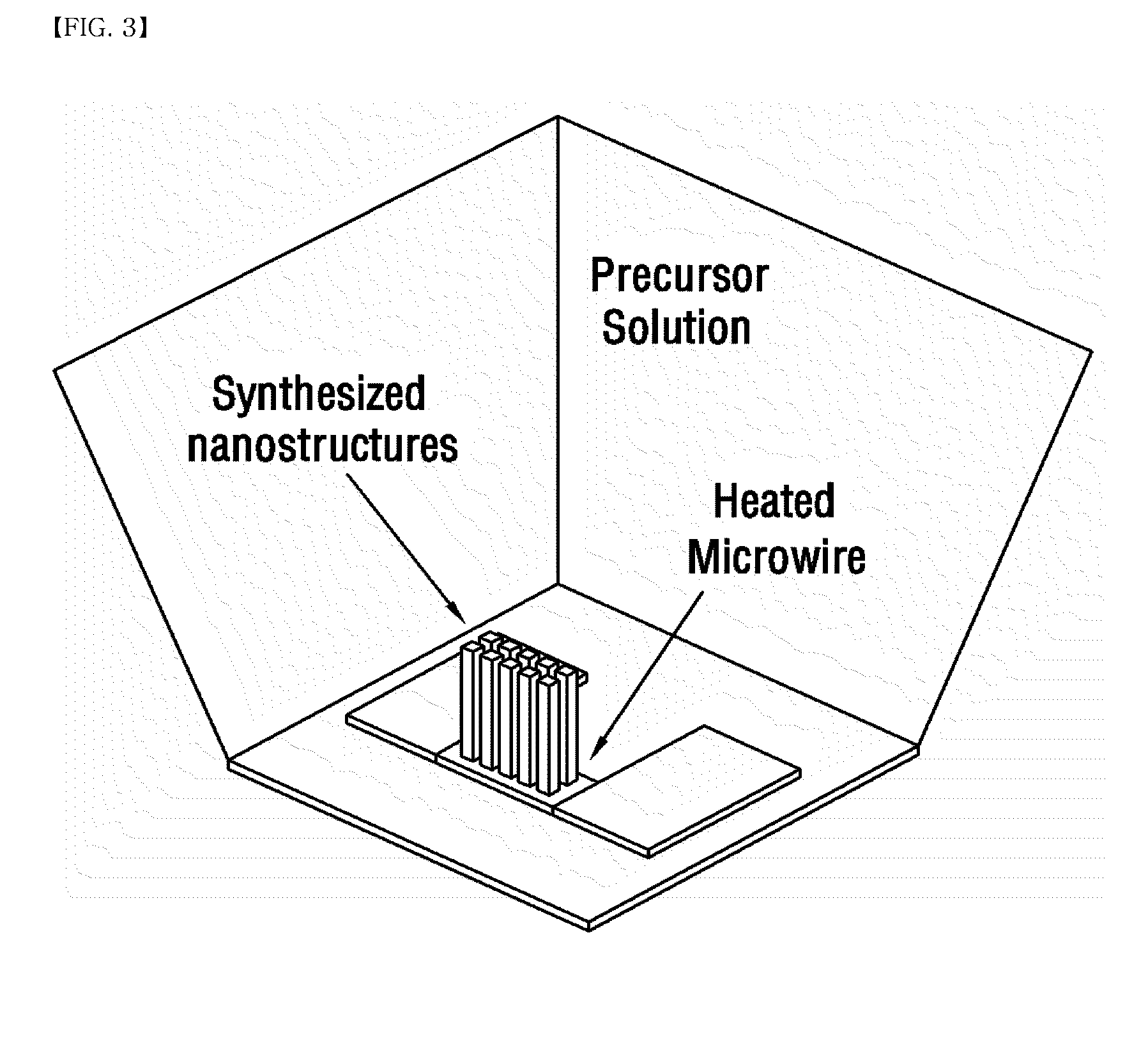
[0054]FIG. 3 is a schematic view illustrating a method for producing nanostructures by using a micro heater in accordance with an embodiment of the present invention.

[0055]Referring to FIG. 3, the method for producing nanostructures according to an embodiment of the present invention allows the nanostructures to grow in a bottom-up mode under the liquid environment of a precursor solution, unlike vapor-liquid-solid (VLS) performed in a vapor phase by evaporating precursor materials, etc. Thus, an embodiment of the present invention is based on the finding that when growing nanostructures by heating a precursor solution locally and selectively with a heater, the growth of nanostructures and the location thereof are controlled by the heater. In this case, the initial generation, growth, integration, etc. of the nanostructures may be carried out in a one-step mode.

[0056]FIG. 4 is a flow chart of the method for producing nanostructures acco...

example 2

Method for Producing Nanostructures by Photon Energy

[0090]In another embodiment of the present invention, nanowires are grown in a liquid phase by concentrating photon energy at a specific point of a substrate.

[0091]In this manner, nanostructures are grown from a desired point by heating a specific point of a device without any additional patterning step, unlike the prior art that requires patterning of a seed layer or micro heater on a so that the nanostructures may be grown at the point. Further, according to the prior art, a patterning process including exposure and development is performed to define the point, where the nanostructures are to be grown, or a heater is provided. Thus, it is difficult to grow nanostructures with high precision. Moreover, it is required to recover the grown nanostructures and to assemble them precisely. On the contrary, in this embodiment, photon energy such as laser capable of precise control is used to grow nanostructures directly on a random posit...


PUM

PropertyMeasurementUnit
Temperatureaaaaaaaaaa
Electrical conductoraaaaaaaaaa
Boiling pointaaaaaaaaaa

Abstract

Provided are methods for producing nanostructures and nanostructures obtained thereby. The methods include heating a certain point of a substrate dipped into a precursor solution of the nanostructures so that the nanostructures are grown in a liquid phase environment without evaporation of the precursor solution. The methods show excellent cost-effectiveness because of the lack of a need for precursor evaporation at high temperature. In addition, unlike the vapor-liquid-solid (VLS) process performed in a vapor phase, the method includes growing nanostructures in a liquid phase environment, and thus provides excellent safety and eco-friendly characteristics as well as cost-effectiveness. Further, the method includes locally heating a substrate dipped into a precursor solution merely at a point where the nanostructures are to be grown, so that the nanostructures are grown directly at a desired point of the substrate. Therefore, it is possible to grow and produce nanostructures directly in a device. As a result, unlike the conventional process, it is not necessary to assemble and integrate the nanostructures produced in a sacrificial substrate into a device.

Description

CROSS-REFERENCE(S) TO RELATED APPLICATIONS[0001]The present invention claims priority of Korean Patent Application Nos. 10-2009-0061510 filed on Jul. 7, 2009 and 10-2010-0013750 filed on Feb. 16, 2010, which are incorporated herein by reference.BACKGROUND OF THE INVENTION[0002]1. Field of the Invention[0003]The present invention relates to a method for producing nanostructures and nanostructures obtained by the same method. More particularly, the present invention relates to a method for producing nanostructures having a desired shape easily with excellent cost-efficiency and safety by allowing nanostructures to grow in a liquid phase environment, unlike a conventional vapor-liquid-solid (VLS) process performed in a vapor phase, as well as to nanostructures obtained by the same method.[0004]2. Description of Related Art[0005]NEMS is the abbreviation of nanoelectromechanical systems and refers to the field of nano-scaled ultra-compact precision machines smaller than microelectromecha...

Claims


Application Information

Patent Timeline
IPC IPC(8): C01G9/02C01G39/02C01G29/00C01G19/02C01G31/02C01G45/02C01G49/02B05D3/06B05D1/18
CPCB81B2201/0214G01J1/429B82Y15/00B82Y30/00B82Y40/00C01G9/02C01G19/02C01G21/21C01G29/00C01G31/02C01G39/02C01G41/02C01G45/02C01G51/00C01P2002/84C01P2004/03C01P2004/16C30B7/00C30B7/10C30B29/16C30B29/60B81C1/00341
Inventor PARK, INKYUKO, SEUNG HWAN
Owner KOREA ADVANCED INST OF SCI & TECH
Why Eureka
Try Eureka