
Microchip and Method of Manufacturing Same

a microchip and manufacturing method technology, applied in the field of microchips, can solve the problems of difficult balance of sufficient joint strength and a solution, difficult to accurately analyze, and difficult to achieve accurate analysis, so as to prevent the reduction of flow rate, the effect of suppressing the variation of cross section and accurate analysis

Inactive Publication Date: 2011-01-20
KONICA MINOLTA OPTO
View PDF3 Cites 2 Cited by
  • Summary
  • Abstract
  • Description
  • Claims
  • Application Information

AI Technical Summary

Benefits of technology

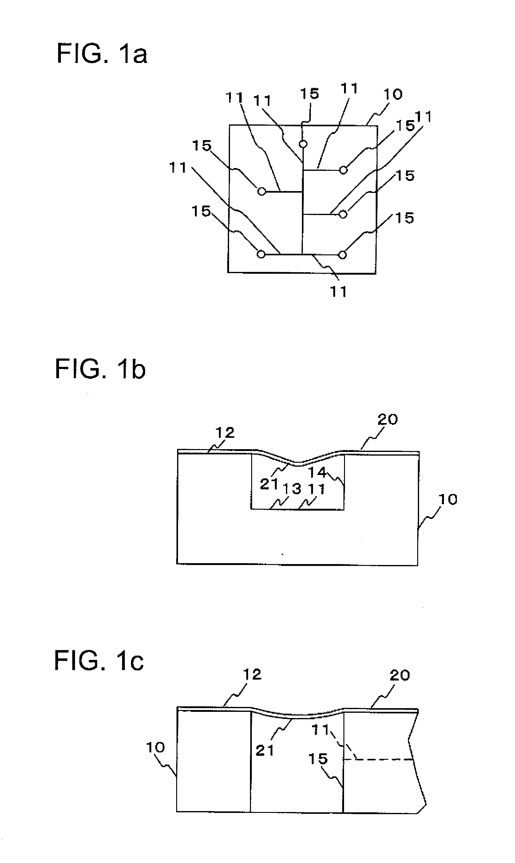
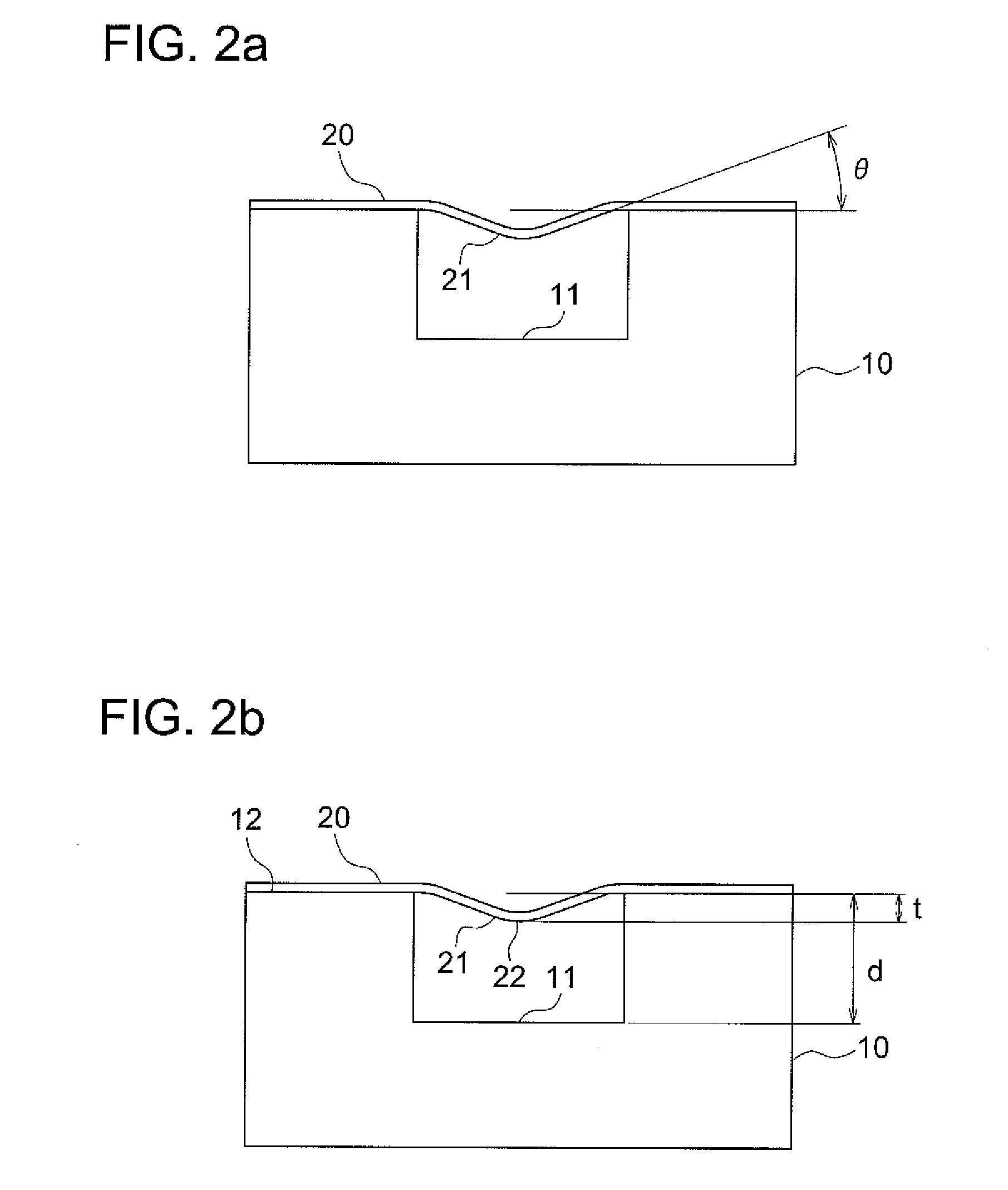
[0028]According to the invention described in claims 1 and 2, since the acute angle made by the deflected section of the resin film in the flow path and the surface of the wall of the flow path groove becomes larger, the flow rate of the liquid sample is not partially decreased at the acute angle portion, whereby stagnation of the liquid sample is controlled, and as a result, the liquid sample can be accurately analyzed.
[0029]According to the invention described in claims 3 and 4, the cross section of the flow path does not become small, as well as the suppression of variation of the cross section, whereby the decrease in flow rate is prevented, and as a result, it becomes possible to prevent decrease in reproducibility of detection.
[0030]According to the invention described in claims 5 and 6, the variation of volume of the through-hole can be suppressed, resulting in the variation of height of the surface of a liquid filled in the through-hole, for example the liquid sample, being suppressed, and thereby it becomes possible to improve the quantitative capability of the liquid sample. Further, it becomes possible to stop generation of a water head difference between a liquid sample of a through-hole and a liquid sample of the other through-hole, thereby it becomes possible to prevent a flow of the liquid sample originated from the head difference.
[0031]According to the invention described in claim 7, when the thermal annealing is carried out after the resin film is joined to the resin substrate, the resin film shrinks, thereby it becomes possible to suppress the deflection of the resin film at the flow path.
[0032]According to the invention described in claim 8, when the thermal annealing is carried out after the resin film is joined to the resin substrate, the resin film shrinks, thereby it becomes possible to suppress the deflection of the resin film at the through-hole.
[0033]According to the invention described in claim 9, since the pin supports the resin film deflecting toward the through-hole when the resin film is joined to the resin substrate, the deflection of the resin film at the through-hole can be decreased or eliminated.

Problems solved by technology

However, when a microchip was formed by thermally fusion-bonding a resin substrate to a resin film according to a content described in the above patent document, and the formed microchip was analyzed, a problem was found that a variation of the flow rate of chemical reagent arose, resulting in a difficulty of an accurate analysis.
It was also found that, when detection was carried out with detection light, the detection light diverged, resulting in a weak detection peak, thereby another problem that an accurate analysis became difficult was caused.
However, for these problems, it was difficult to balance the sufficient joint strength and a solution of the above-described problem, even if conditions such as press pressure or temperature during thermal fusion-bonding were changed.

Method used


Image

  • Microchip and Method of Manufacturing Same
  • Microchip and Method of Manufacturing Same
  • Microchip and Method of Manufacturing Same

Examples


example 1

(Joining of Resin Substrate 10 to Resin Film 20, and Thermal Annealing)

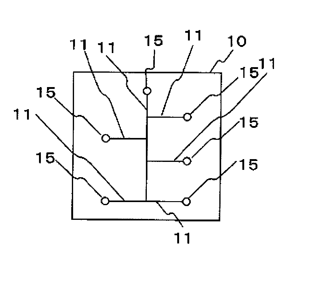
[0110]Next, Example 1 will be described. An acrylic resin such as polymethyl methacrylate, which is a transparent resin material, (DELPET 70 NH, manufactured by Asahi Kasei Corp.) was molded using an injection molding machine to manufacture the resin substrate 10, which was constituted of the plural flow path grooves 11 of 50 μm in width and 50 μm in depth and the plural through-holes of 2 mm in internal diameter, on a plate-like member of 50 mm×50 mm×1 mm in external dimensions.

[0111]As the resin film 20, an acrylic resin such as polymethyl methacrylate, which is a transparent resin material, (ACRYPLENE, 75 μm in thickness, manufactured by Mitsubishi Rayon Co., Ltd.), was cut into 50 mm×50 mm. Then, the resin film 20 was placed on the joint surface 12 of the resin substrate 10 on which the flow path grooves 11 were formed, which were then pressure bonded using a heat press at press temperature of 90° C. and with...

example 2

(Joining of Resin Substrate 10 to Resin Film 20, and Thermal Annealing)

[0113]Next, Example 2 will be described. An acrylic resin such as polymethyl methacrylate, which is a transparent resin material, (DELPET 70 NH, manufactured by Asahi Kasei Corp.) was molded using an injection molding machine to manufacture the resin substrate 10, which was constituted of the plural flow path grooves 11 of 50 μm in width and 50 μm in depth and the plural through-holes of 2 mm in internal diameter, on a plate-like member of 50 mm×50 mm×1 mm in external dimensions.

[0114]As the resin film 20, an acrylic resin such as polymethyl methacrylate, which is a transparent resin material, (ACRYPLENE, 75 μm in thickness, manufactured by Mitsubishi Rayon Co., Ltd.), was cut into 50 mm×50 mm. Then, the resin film 20 was placed on the joint surface 12 of the resin substrate 10 on which the flow path grooves 11 were formed, which were then pressure bonded using a heat press at press temperature of 90° C. and with...

example 3

(Joining of Resin Substrate 10 to Resin Film 20, and Thermal Annealing)

[0116]Next, Example 3 will be described. An acrylic resin such as polymethyl methacrylate, which is a transparent resin material, (DELPET 70 NH, manufactured by Asahi Kasei Corp.) was molded using an injection molding machine to manufacture the resin substrate 10, which was constituted of the plural flow path grooves 11 of 50 μm in width and 50 μm in depth and the plural through-holes of 2 mm in internal diameter, on a plate-like member of 50 mm×50 mm×1 mm in external dimensions.

[0117]As the resin film 20, an acrylic resin such as polymethyl methacrylate, which is a transparent resin material, (ACRYPLENE, 75 μm in thickness, manufactured by Mitsubishi Rayon Co., Ltd.), was cut into 50 mm×50 mm. Then, the resin film 20 was placed on the joint surface 12 of the resin substrate 10 on which the flow path grooves 11 were formed, which were then pressure bonded using a heat press at press temperature of 90° C. and with...


PUM

PropertyMeasurementUnit
deflection angleaaaaaaaaaa

Abstract

Provided are a microchip enabling accurate analysis by preventing a resin film from being deflected into a flow path groove to eliminate the stagnation of a liquid sample and a method of manufacturing the microchip. This microchip includes a flow path that is formed by joining a resin film onto the groove-formed surface of a resin substrate. The deflection angle of the resin film in the sectional surface of the flow path in the width direction is made to be 0 to less than 30° at respective positions of the flow path.

Description

TECHNICAL FIELD[0001]The present invention relates to a microchip having a flow path and a method for manufacturing the same.BACKGROUND TECHNOLOGY[0002]There has been practically used a device, called a microanalysis chip or μTAS (Micro Total Analysis Systems), which carries out a chemical reaction, separation, or analysis of a liquid sample such as a nucleic acid, protein, and blood, on a minute space, which is created in such a way that minute flow path grooves are formed on a silicon or glass substrate using the micromachining technology, and then, a flow path or a circuit is formed by joining a tabular seal member to the aforesaid substrate. The merit of such a microchip may be to realize a small, portable and inexpensive system, in which an amount of sample or reagent to be used or an amount of emission of waste liquid are reduced.[0003]In addition, from a demand for a reduction in a manufacturing cost, it has also been studied that the microchip is manufactured using a resin s...

Claims


Application Information

Patent Timeline
Patent Type & Authority Applications(United States)
IPC IPC(8): B32B3/10B32B3/30B32B37/00B32B38/04
CPCB01L3/502707B01L3/502746B01L2200/0689B01L2300/0816B01L2300/0887B81B2201/058Y10T156/1062B81B2203/0384B81C1/00103B81C2201/019Y10T428/24331Y10T428/24562B81B2203/0338
Inventor HIRAYAMA, HIROSHI
Owner KONICA MINOLTA OPTO
Learn More