Luminous device

a technology of semiconductor diodes and luminous devices, which is applied in the direction of discharge tubes/lamp details, discharge tubes/lamp details, etc., can solve the problems of increasing the etendue of semiconductor diodes, reducing the generated light flux, and reducing so as to increase the amount of red, increase the efficiency of luminous devices, and increase the effect of extraction efficiency

Inactive Publication Date: 2011-02-03
KONINKLIJKE PHILIPS ELECTRONICS NV
View PDF10 Cites 83 Cited by
  • Summary
  • Abstract
  • Description
  • Claims
  • Application Information

AI Technical Summary

Benefits of technology

[0020]In further embodiments of the luminous device according to the present invention, the output section comprises a roughened area, such as a forward scattering area or a forward scattering layer / coating, micro-optical extraction structures, micro-prismatic pyramids or grooves, diffraction gratings, holographic grating structures, photonic crystals, quasi-photonic crystals or the like or a combination thereof. In this manner, the extraction efficiency of the luminous device may be increased.
[0021]In yet further embodiments of the luminous device according to the present invention, the light emitting element (or light transmissive assembly) further comprises a light guiding layer, disposed between the semiconductor diode and the output section. For example, the light guiding layer may comprise a phosphor material, a phosphor ceramic material, an LED substrate, transparent YAG, glass, sapphire, alumina or quartz, or a combination thereof. In case the light guiding layer comprises a phosphor material and a transparent layer (an LED substrate), the total thickness of the phosphor material and the transparent layer may be tuned to the thickness of the active light generating layer of the semiconductor diode. In this manner, the efficiency of the device may, in general, be increased provided that the light guiding layer is substantially non-lossy and non-absorbing.
[0022]In yet other embodiments of the luminous device according to the present invention, the output section is provided with a first phosphor (ceramic) material. In this manner, color content of light emitted from the luminous device may be controlled.
[0023]Furthermore, in still other embodiments of the luminous device according to the present invention, a phosphor (ceramic) material, provided at the output section, may be of a different type than a phosphor (ceramic) material comprised by the light guiding layer. For example, a luminous device comprising a semiconductor diode emitting blue light, a light guiding layer of a phosphor material, such as YAG:Ce (converting blue light to green, yellow and some red light), resulting in a white (i.e. a mixture of red, green and blue) light flux, and an output section comprising a red phosphor material may provide a warm white light emission. A portion of the blue light will be converted to red, yellow and green light in the white phosphor (thereby providing white light as a mixture of red, yellow, green and blue) and the red phosphor will increase the amount of red in the emitted light such that the emitted light will be perceived as warm white light (i.e. white light having a red component).

Problems solved by technology

However, merely reducing the size of the semiconductor diode by scaling down the entire semiconductor diode reduces the generated light flux.
For instance, light emitted towards the edges of a device or backwards towards reflectors surrounding the semiconductor diode is usually difficult to use in collimating optics and increases the etendue of the semiconductor diode.
Disadvantageously, the efficiency of the luminous element is poor.

Method used


Image

  • Luminous device
  • Luminous device
  • Luminous device

Examples


Embodiment Construction

[0044]Throughout the following description similar reference numerals have been used to denote similar elements, parts, items or features, when applicable.

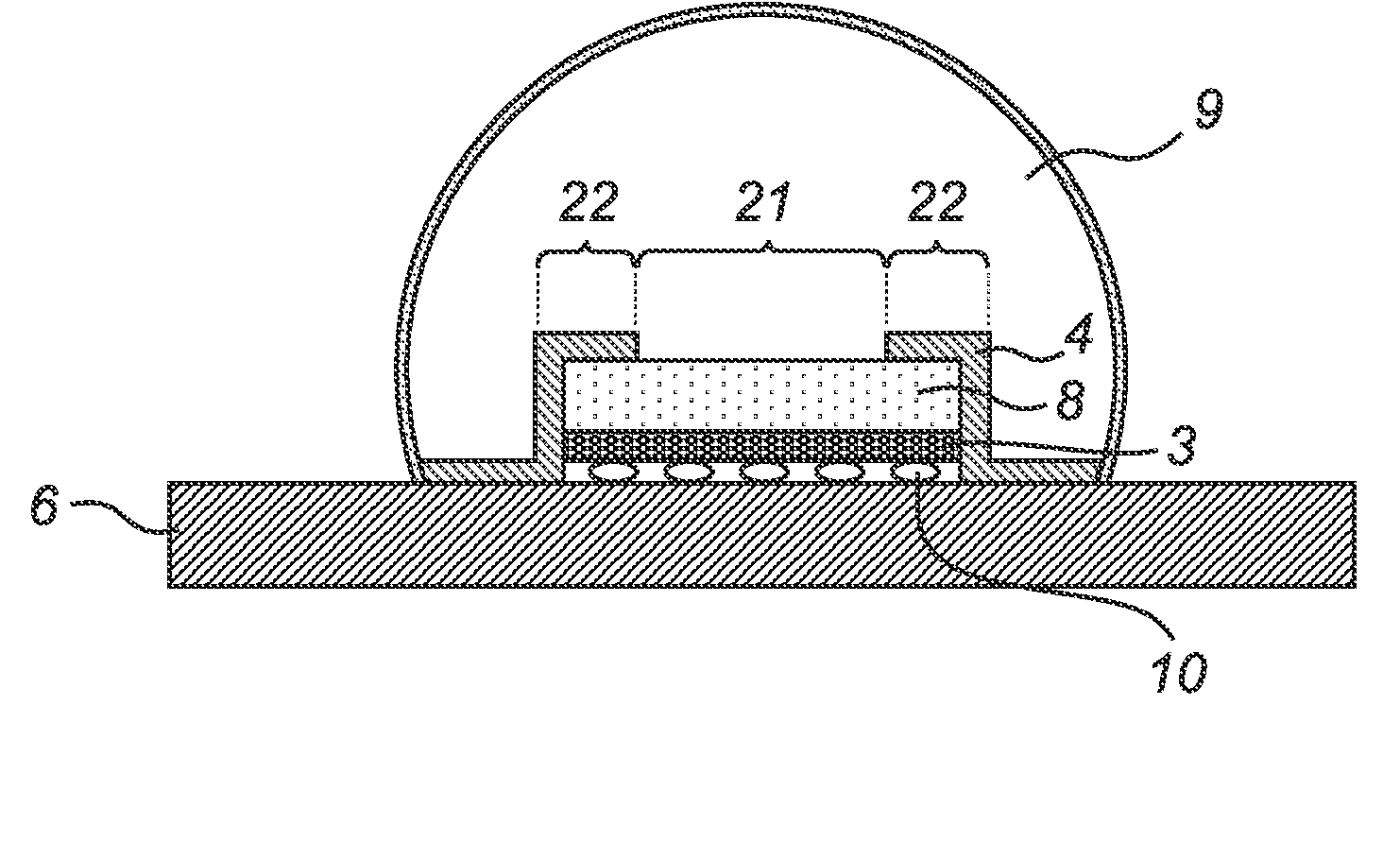
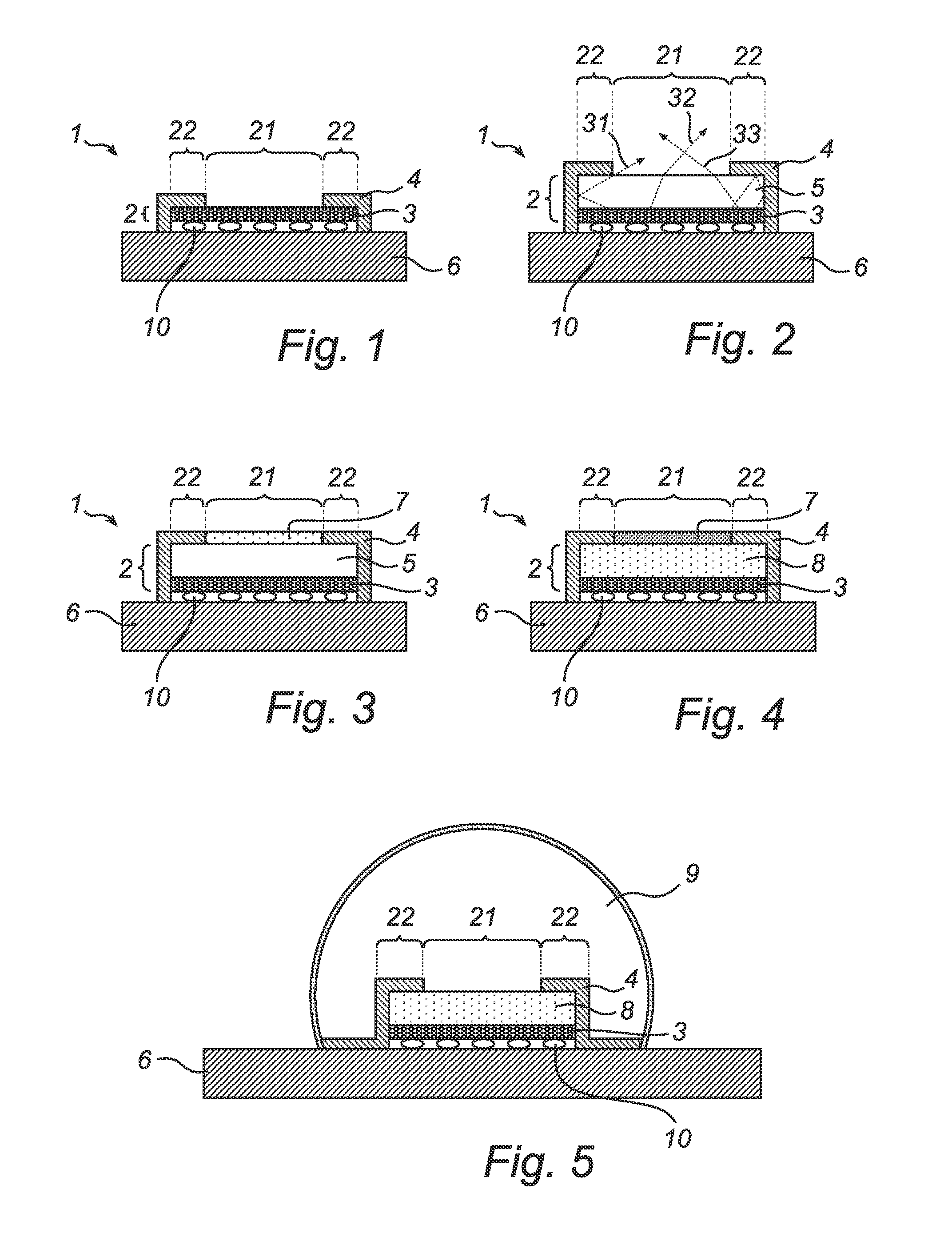
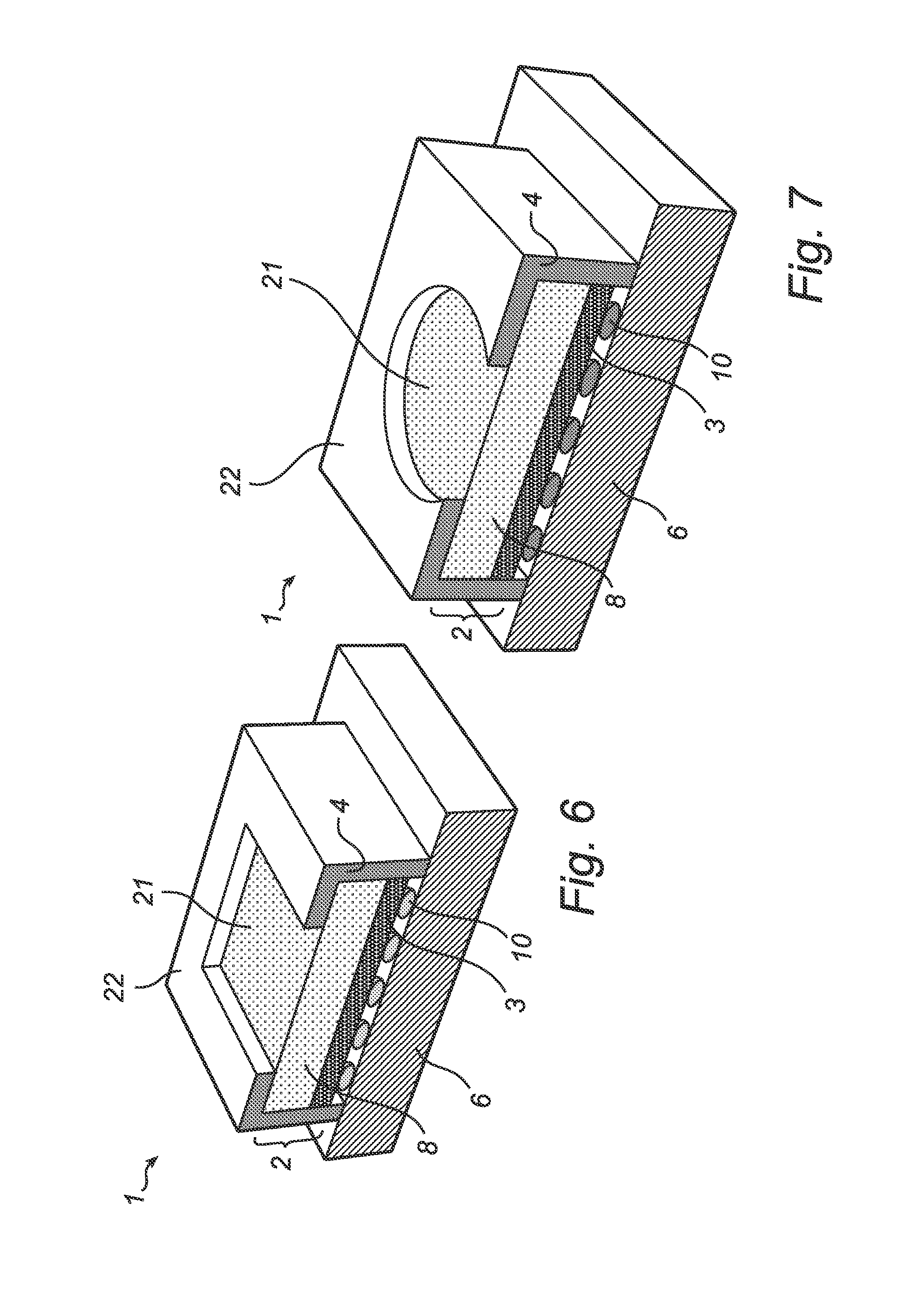
[0045]In FIG. 1, there is shown a cross-sectional, side view of a luminous device according to an embodiment of the present invention. The luminous device 1 comprises a light transmissive element 2, which in this case is an LED die or LED chip 3, and a reflector 4 (a reflecting structure). The luminous device is mounted on a submount 6. As can be seen from FIG. 1, the reflector 4 is arranged to partially cover the upper surface of the LED die 3. As a result, the upper (according to FIG. 1) surface of the LED die 3 (LED layer or semiconductor diode structure) comprises an output section 21 for outputting light from the LED die 3 and a reflecting section 22 for reflecting light from the LED die 3 back into the LED die. The reflected light will be reflected once again and will eventually hit the output section 21, thereby contributin...


PUM


Abstract

The present invention relates to the field of luminous devices, in particular to a luminous device (1) comprising a light transmissive element (2). The light transmissive element further comprises a semiconductor diode structure (3) for generating light, a reflecting section (22) for reflecting light from the diode structure (3) into the light transmissive element (2) and an output section (21) for outputting light from the diode structure (3). The luminous device (1) further comprises a reflecting structure (4), at least partially enclosing side surfaces of the light transmissive element (2), for reflecting light from the diode structure (3) towards the output section (21).

Description

FIELD OF THE INVENTION[0001]The present invention relates to the field of semiconductor luminous devices, more particularly to a luminous device comprising a light transmissive element, which comprises a semiconductor diode structure for generating light.BACKGROUND OF THE INVENTION[0002]Semiconductor diodes, such as light emitting diodes (LEDs), high power LEDs, organic light emitting diodes (OLEDs) and laser diodes, are known to be energy efficient and small light sources that have a small etendue (i.e. the product of emitting area with solid angle in which the light is emitted). This implies that these diodes emit light from a relatively small area into a limited angular range, such as a half sphere. By using semiconductor diodes small and efficient optical systems may be built. Such optical systems typically collimate / direct light for further processing as required by any specific application. Typical examples of applications are projection systems, automotive front lighting, cam...

Claims


Application Information

Patent Timeline
Patent Type & Authority Applications(United States)
IPC IPC(8): H01J1/62H01J5/16H01L33/22H01L33/30H01L33/38H01L33/50H01L33/58H01L33/60
CPCH01L33/22H01L33/30H01L33/504H01L2224/13H01L33/58H01L33/60H01L33/508
Inventor JAGT, HENDRIK JOHANNES BOUDEWIJN
Owner KONINKLIJKE PHILIPS ELECTRONICS NV
Why Eureka
Try Eureka