

Solid-state image pickup element and a method of manufacturing the same, and image pickup device including the same
a pickup element and solid-state technology, applied in the direction of color signal processing circuits, television system scanning details, television systems, etc., can solve the problem of not wanting to hold high temperature for a long time, suppress the generation of dark current caused by the interface state, and reduce the production cost.
- Summary
- Abstract
- Description
- Claims
- Application Information
AI Technical Summary
Benefits of technology
Problems solved by technology
Method used
Image

Examples
Embodiment Construction
[0042]The preferred embodiments of the present invention will be described in detail hereinafter with reference to the accompanying drawings.
[0043]It is noted that the description will be given below in accordance with the following order.
[0044]1. Outline of the Present Invention
[0045]2. Solid-State Image Pickup Element
[0046]3. Method of Manufacturing Solid-State Image Pickup Element
[0047]4. Experiments (Measurements of Characteristics)
[0048]5. Image Pickup Device
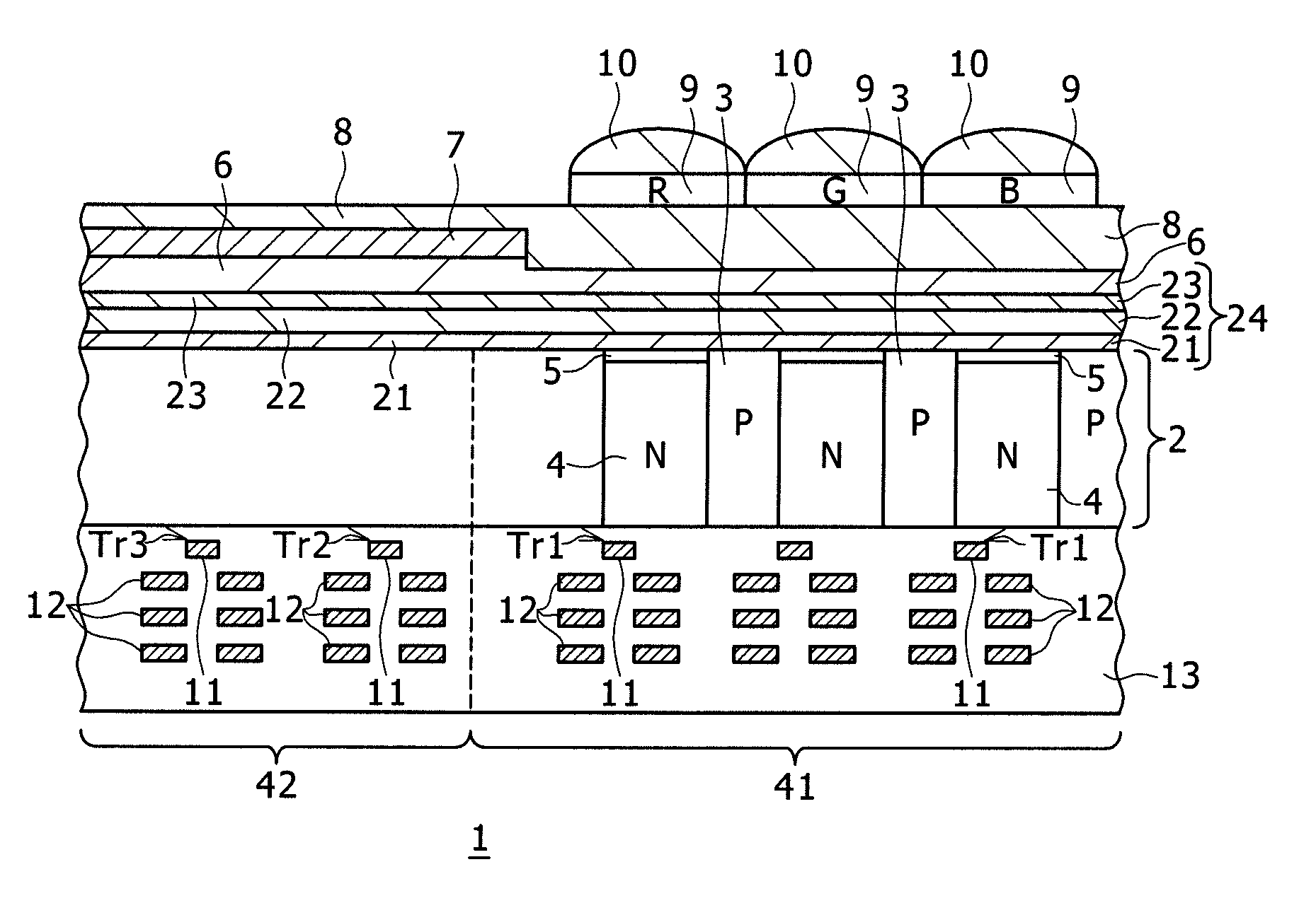
1. Outline of the Present Invention
[0049]In the present invention, a first film containing therein negative fixed charges is formed on a semiconductor layer in a region in which at least a photodiode of a solid-state image pickup element is formed, and a second film containing therein the negative fixed charges is formed on the first film. In addition, a third film containing therein the negative fixed charges is formed on the second film.
[0050]The first film is formed (deposited) by utilizing either an Atomic Layer Deposit...
PUM
 Abstract
Description
Claims
Application Information