Printed circuit board and electro application

a printed circuit board and electro-application technology, applied in the direction of printed circuit non-printed electric components association, coupling device connection, waveguide, etc., can solve the problems of emi, a serious problem, and a desperate need for a solution, so as to improve the efficiency of manufacturing, facilitate the application of various frequencies, and reduce the effect of manufacturing cos

Active Publication Date: 2011-02-03
SAMSUNG ELECTRO MECHANICS CO LTD
View PDF70 Cites 25 Cited by
  • Summary
  • Abstract
  • Description
  • Claims
  • Application Information

AI Technical Summary

Benefits of technology

The present invention provides a printed circuit board and an electronic product that can readily absorb various frequencies, be easily applied without any antenna effect and be cost-effective in manufacturing.

Problems solved by technology

As the operating frequencies of electronic products become higher, electromagnetic interference (EMI) has been perceived as a chronic noise problem.
Particularly, the operating frequencies of electronic products have reached a few ten MHz, or even a few GHz, making the EMI problems more serious.
Subsequently, finding a solution to the problems is desperately needed.
Among the EMI problems occurring at a board, a solution for the noise problems particularly occurred at the edge of the board has not been sufficiently researched, making it difficult to completely block the noise at the board.
EMI noise refers to a noise that creates a noise problem caused by interference when an electromagnetic (EM) wave generated in one electronic circuit, component or part is transferred to another electronic circuit, component or part.
However, in the case of using the shield can 40, since a new radiation noise 10′ is generated due to the antenna effect, it is difficult to shield all EMI noises radiated towards the outside of the board, and there are limitations to frequency ranges that can be absorbed by the EMI field absorber 42, making it urgently needed to find an effective shielding method.
Furthermore, not only is the thickness of the shield can restricted, but also the shield can increases the weight of a lightweight electronic device.
Also, in the case of the EMI field absorber 42, it is difficult to develop a material that can shield the EMI noise in various frequencies, and it may take longer to develop the material, thereby increasing the production cost.

Method used


Image

  • Printed circuit board and electro application
  • Printed circuit board and electro application
  • Printed circuit board and electro application

Examples


Embodiment Construction

As the invention allows for various changes and numerous embodiments, particular embodiments will be illustrated in the drawings and described in detail in the written description. However, this is not intended to limit the present invention to particular modes of practice, and it is to be appreciated that all changes, equivalents, and substitutes that do not depart from the spirit and technical scope of the present invention are encompassed in the present invention. In the description of the present invention, certain detailed explanations of related art are omitted when it is deemed that they may unnecessarily obscure the essence of the invention.

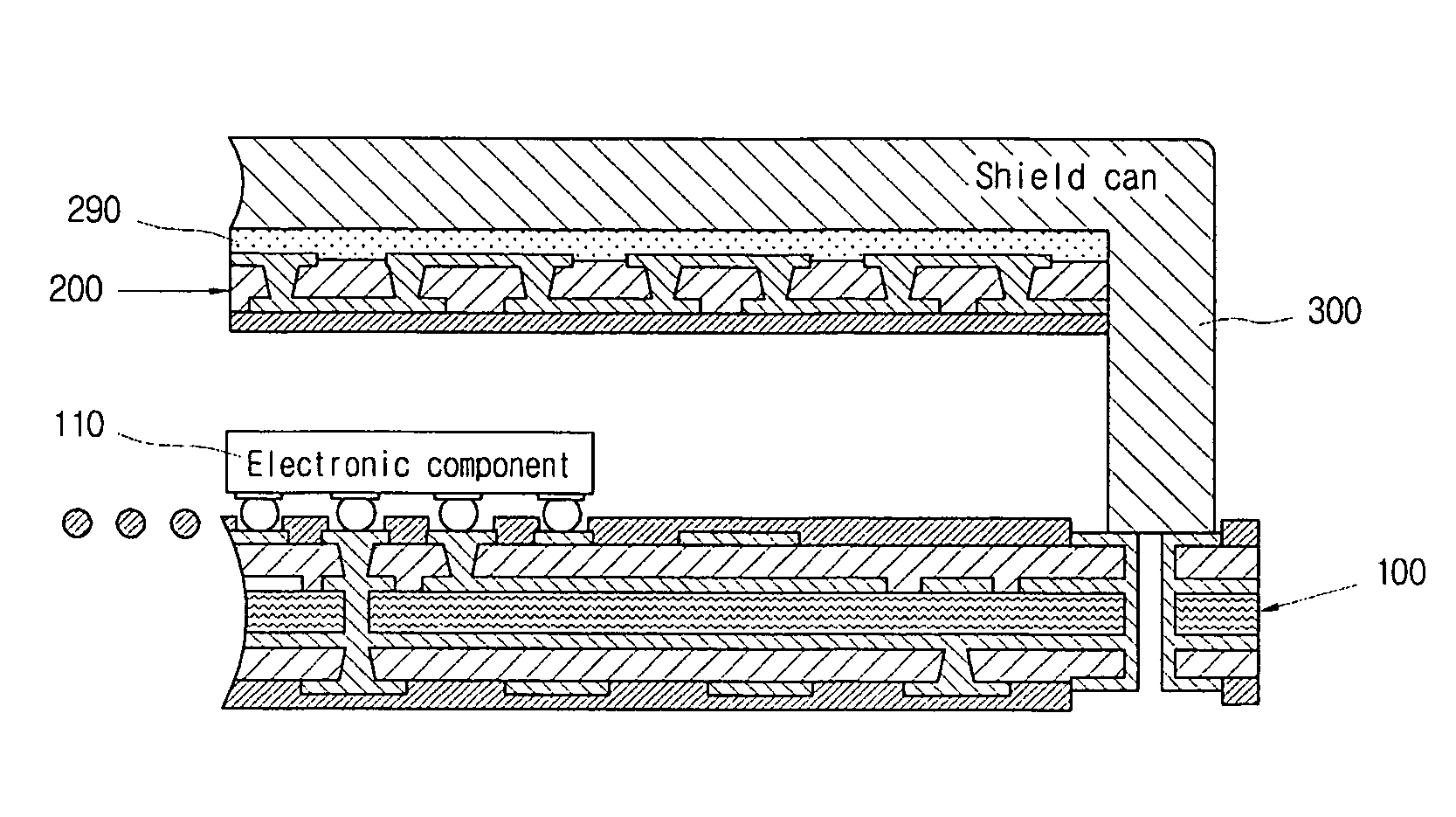
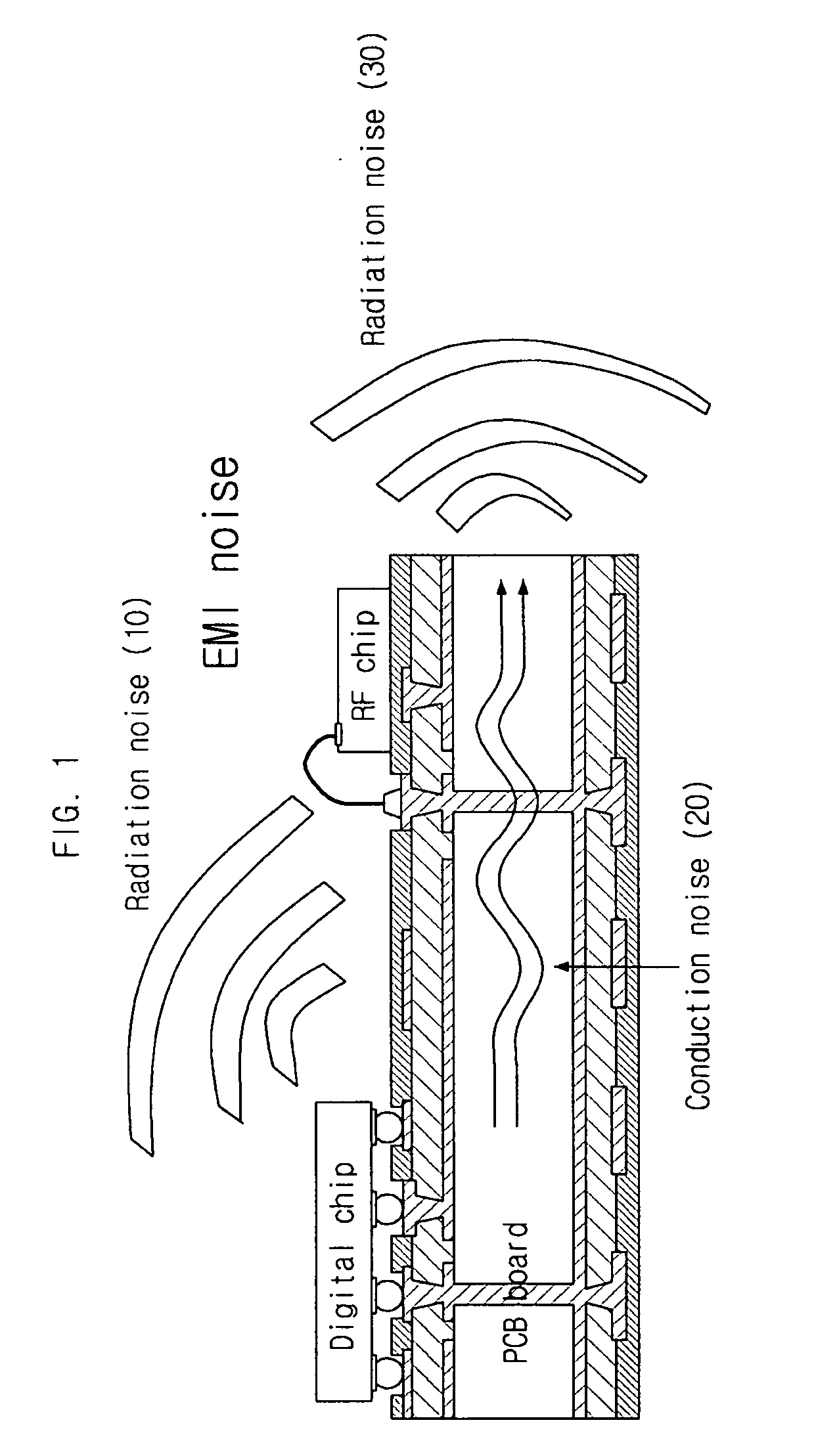
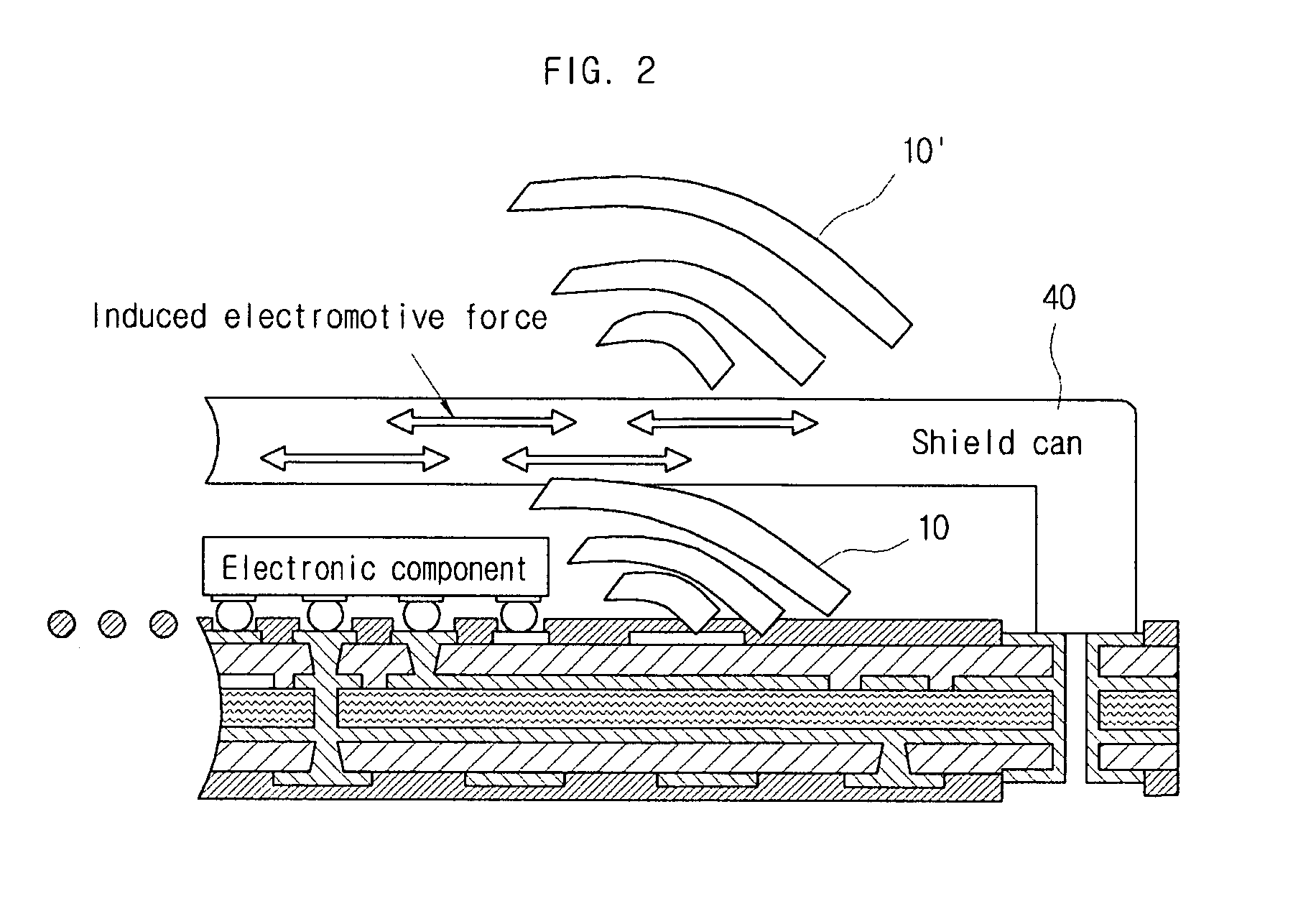
A printed circuit board and an electronic product according to certain embodiments of the present invention will be described below in more detail with reference to the accompanying drawings. Those components that are the same or are in correspondence are rendered the same reference numeral regardless of the figure number, and redundant d...


PUM


Abstract

A printed circuit board and an electronic product are disclosed. In accordance with an embodiment of the present invention, the printed circuit board includes a first board, which has an electronic component mounted thereon, and a second board, which is positioned on an upper side of the first board and covers at least a portion of an upper surface of the first board and in which an EBG structure is inserted into the second board such that a noise radiating upwards from the first board is shielded. Thus, the printed circuit board can readily absorb various frequencies, be easily applied without any antenna effect and be cost-effective in manufacturing.

Description

CROSS-REFERENCE TO RELATED APPLICATIONSThis application claims the benefit of Korean Patent Application No. 10-2009-0069666, filed with the Korean Intellectual Property Office on Jul. 29, 2009, the disclosure of which is incorporated herein by reference in its entirety.BACKGROUND1. Technical FieldThe present invention relates to a printed circuit board and an electronic product.2. Description of the Related ArtAs the operating frequencies of electronic products become higher, electromagnetic interference (EMI) has been perceived as a chronic noise problem. Particularly, the operating frequencies of electronic products have reached a few ten MHz, or even a few GHz, making the EMI problems more serious. Subsequently, finding a solution to the problems is desperately needed. Among the EMI problems occurring at a board, a solution for the noise problems particularly occurred at the edge of the board has not been sufficiently researched, making it difficult to completely block the noise ...

Claims


Application Information

Patent Timeline
Patent Type & Authority Applications(United States)
IPC IPC(8): H05K9/00H05K7/14
CPCH05K1/0236H05K1/144H05K1/183H05K9/0052H05K2201/10371H05K2201/09681H01L2924/3025H01Q1/526H05K1/0224H05K1/0237H05K1/0298H05K9/0009H01L2224/16225H01L2224/16235H01L2224/16237H01L2224/32225H01L2224/48091H01L2224/48227H01L2224/73253H01L2924/15153H01L2924/15192H01L2924/15313H01L2924/16251H05K1/18H05K9/00
Inventor KIM, HANRYU, CHANG-SUP
Owner SAMSUNG ELECTRO MECHANICS CO LTD
Why Eureka
Try Eureka