Semiconductor device manufacturing method and semiconductor device

Active Publication Date: 2011-02-10
KIOXIA CORP
View PDF3 Cites 103 Cited by
  • Summary
  • Abstract
  • Description
  • Claims
  • Application Information

AI Technical Summary

Problems solved by technology

Thus, the metal silicidation process for the memory cell array cannot be directly applied thereto.

Method used


Image

  • Semiconductor device manufacturing method and semiconductor device
  • Semiconductor device manufacturing method and semiconductor device
  • Semiconductor device manufacturing method and semiconductor device

Examples


Embodiment Construction

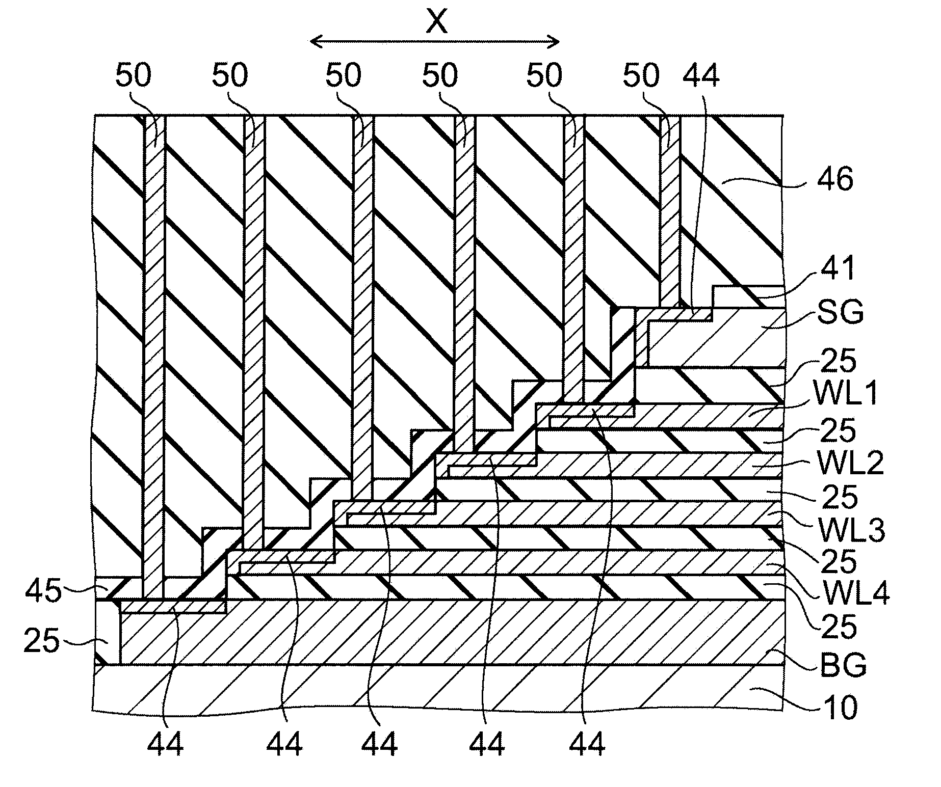
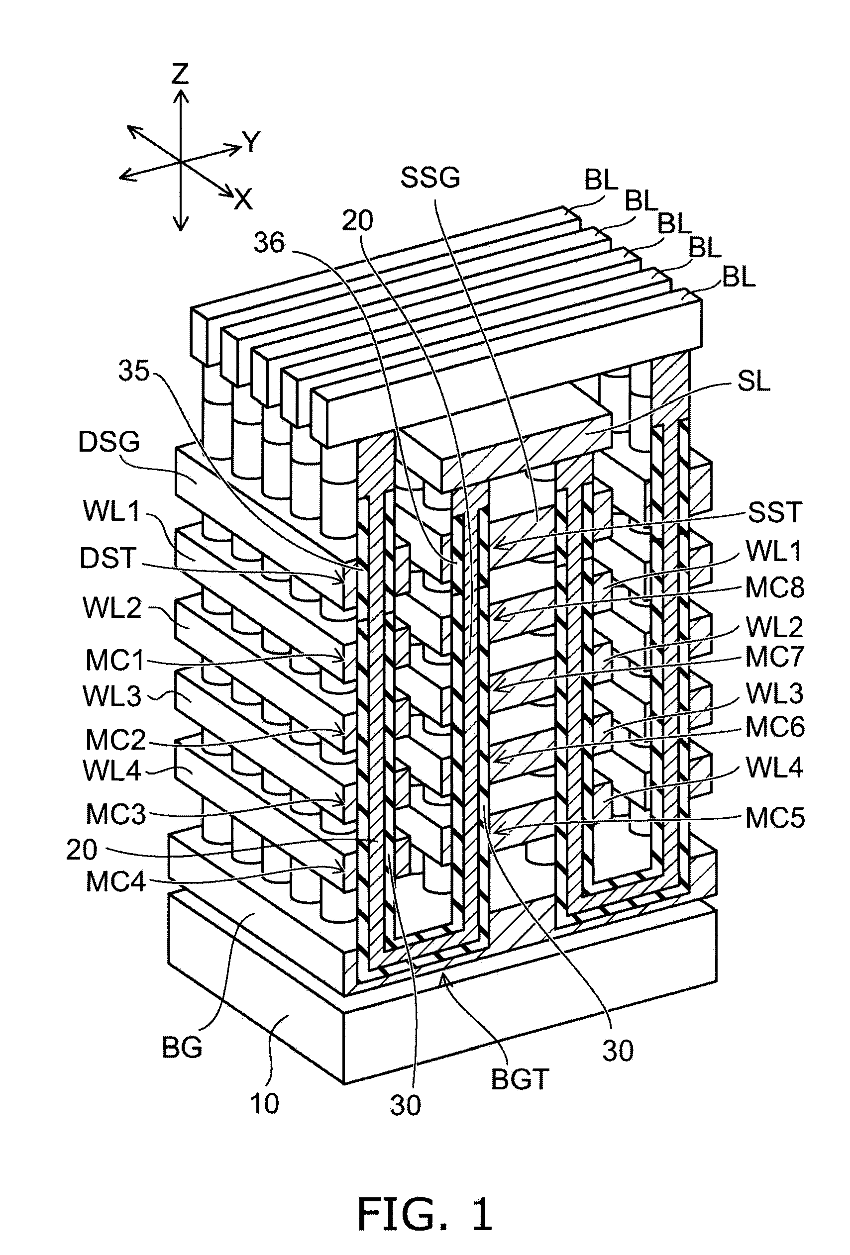
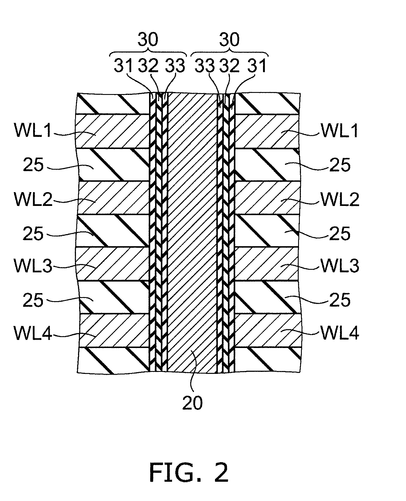
[0015]FIG. 1 is a schematic view illustrating the configuration of a memory cell array in a semiconductor device according to an embodiment of the invention. In FIG. 1, for clarity of illustration, insulating portions are not shown, except insulating films in a memory hole. Although a semiconductor is illustratively silicon in the following embodiments, semiconductors other than silicon may also be used.

[0016]In this specification, for convenience of description, an XYZ orthogonal coordinate system is introduced. In this coordinate system, the two directions parallel to the major surface of a substrate 10 and orthogonal to each other are referred to as X and Y directions, and the direction orthogonal to both the X and Y directions is referred to as a Z direction. A plurality of electrode layers WL1-WL4 are stacked in the Z direction.

[0017]A back gate BG is provided on the substrate 10 via an insulating layer, not shown. The back gate BG is illustratively a silicon layer provided wit...


PUM


Abstract

A semiconductor device manufacturing method includes: stacking a plurality of electrode layers containing a semiconductor alternately with insulating layers; processing part of a multilayer body of the electrode layers and the insulating layers into a staircase shape and exposing a surface of the staircase-shaped electrode layers; forming a metal film in contact with the exposed electrode layers; reacting the semiconductor of the electrode layers with the metal film to form a metal compound in at least a portion of the electrode layers in contact with the metal film; removing an unreacted portion of the metal film; forming an interlayer insulating layer covering the staircase-shaped electrode layers after removing the unreacted portion of the metal film; forming a plurality of contact holes piercing the interlayer insulating layer, each of the contact holes reaching the metal compound of the electrode layer at a corresponding stage; and providing a plurality of contact electrodes inside the contact holes.

Description

CROSS-REFERENCE TO RELATED APPLICATIONS[0001]This application is based upon and claims the benefit of priority from the prior Japanese Patent Application No. 2009-181361, filed on Aug. 4, 2009; the entire contents of which are incorporated herein by reference.BACKGROUND OF THE INVENTION[0002]1. Field of the Invention[0003]This invention relates to a semiconductor device manufacturing method and a semiconductor device.[0004]2. Background Art[0005]A technique for three-dimensionally arranging memory cells is proposed in, for instance, JP-A 2007-180389 (Kokai). In this technique, a plurality of electrode layers functioning as control gates in a memory device are stacked alternately with insulating layers to form a multilayer body, in which silicon pillars are provided via a charge storage layer.[0006]JP-A 2007-180389 (Kokai) also discloses a staircase structure of electrode layers as a structure for connecting each of a plurality of stacked electrode layers to an upper interconnect. In...

Claims


Application Information

Patent Timeline
IPC IPC(8): H01L23/538H01L21/768
CPCH01L27/11582H01L27/11578H10B43/20H10B43/27
Inventor HASHIMOTO, JUNICHI
Owner KIOXIA CORP
Why Eureka
Try Eureka