Electronic device and manufacturing method therefor

a manufacturing method and electronic device technology, applied in the field of electronic devices, can solve the problems of increasing the quantity of solder, increasing the outside dimensions of the formed solder balls, and difficulty in reducing the size (area) of the above bga semiconductor device, so as to improve the reliability (guaranteed quality) reduce the size of the electronic device, and enhance the mounting strength of the electronic device.

Inactive Publication Date: 2011-02-17
RENESAS ELECTRONICS CORP
View PDF1 Cites 34 Cited by
  • Summary
  • Abstract
  • Description
  • Claims
  • Application Information

AI Technical Summary

Benefits of technology

[0011]Attempts have been made to incorporate a wireless communication device into various goods and in recent years, demands for incorporation into mobile goods have also risen. For this reason, the following has been considered to achieve the reduction of the size of a mounting board comprising wireless communication devices and the enhancement of communication speed: placing various components comprising a wireless communication device in one semiconductor device, or so-called modularization.
[0028]The mounting reliability of an electronic device can be enhanced.

Problems solved by technology

However, increase in the quantity of solder also increases the outside dimensions of the formed solder balls.
For this reason, it is difficult to reduce the size (area) of the above BGA semiconductor device.

Method used


Image

  • Electronic device and manufacturing method therefor
  • Electronic device and manufacturing method therefor
  • Electronic device and manufacturing method therefor

Examples


first embodiment

[0072]This embodiment is a semiconductor module for building a wireless communication system such as a wireless LAN.

[0073]

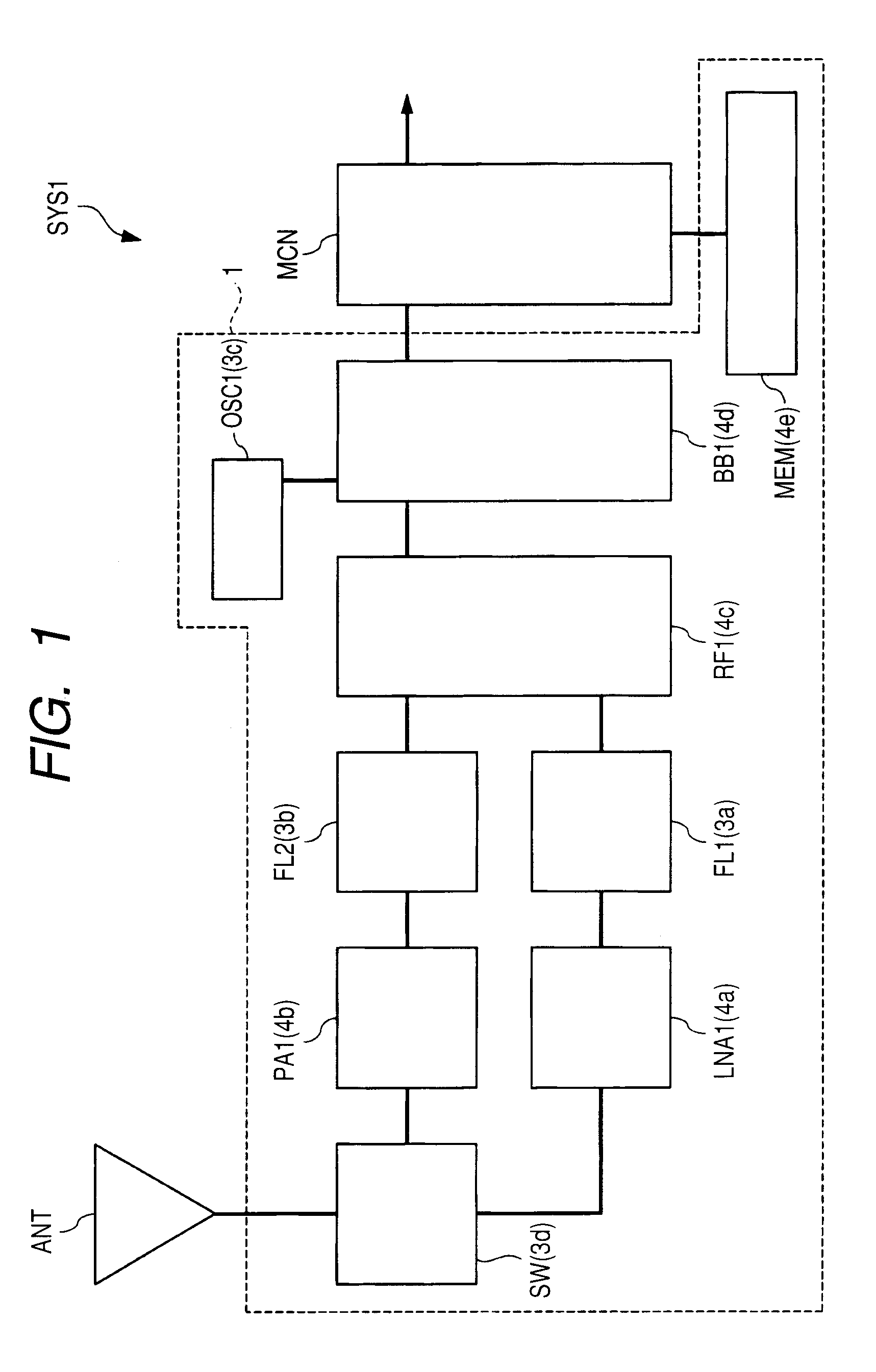
[0074]FIG. 1 is a block diagram (circuit block diagram, explanatory drawing) illustrating an example of an ordinary wireless communication system (for example, wireless LAN) SYS1.

[0075]In the wireless communication system (wireless communication device) SYS1 illustrated in FIG. 1, a signal (radio frequency signal) received via an antenna ANT is passed via an antenna switch SW and is amplified by a low noise amplifier LNA1. It then goes via a filter FL1 for removing unwanted frequencies and is inputted to a high-frequency IC circuit portion RF1. It is there subjected to frequency conversion and demodulated to a base band signal and guided to a base band portion BB1. In the base band portion BB1, there are incorporated an A-D conversion circuit, a D-A conversion circuit, a channel CODEC, DSP (Digital Signal Processor), and the like. The base band signal inputted fr...


PUM


Abstract

Reduction of the size of and enhancement of the reliability, mounting strength, and mounting reliability of a semiconductor module are achieved. The semiconductor module includes: a wiring substrate; an electronic component placed over the upper surface of the wiring substrate; an electronic component placed over the under surface of the wiring substrate; a lead placed over the under surface of the wiring substrate; and encapsulation resin covering the under surface of the wiring substrate including the electronic component and the lead. The lead includes: a first portion coupled to an electrode pad via a joining material; a second portion bent from the first portion; and a third portion bent from the second portion. The third portion is positioned closer to the peripheral edge portion side of the under surface of the wiring substrate than the first portion. At the same time, the third portion is arranged at a position farther from the under surface of the wiring substrate than the first portion. The third portion of the lead is exposed from the main surface and side surface of the encapsulation resin and functions as a terminal for external coupling.

Description

CROSS-REFERENCE TO RELATED APPLICATIONS[0001]The disclosure of Japanese Patent Application No. 2009-187214 filed on Aug. 12, 2009 including the specification, drawings and abstract is incorporated herein by reference in its entirety.BACKGROUND OF THE INVENTION[0002]The present invention relates to electronic devices and manufacturing methods therefor and in particular to a technology effectively applicable to an electronic device obtained by placing an electronic component over a wiring substrate and a manufacturing method therefor.[0003]For example, electronic equipment for carrying out wireless communication is formed by placing the following various components over a mounting board (mother board): an antenna member, a semiconductor device for controlling signals, a crystal resonator, a resistance element, a capacitive element, and the like.[0004]Japanese Unexamined Patent Publication No. Hei 11 (1999)-163249 (Patent Document 1) describes a technology related to a semiconductor de...

Claims


Application Information

Patent Timeline
Patent Type & Authority Applications(United States)
IPC IPC(8): H01L23/485H01L21/50
CPCH01L21/561H01L2924/01033H01L23/3121H01L23/49827H01L23/49861H01L24/16H01L24/48H01L24/97H01L25/16H01L2224/16H01L2224/48091H01L2224/49175H01L2224/97H01L2924/01004H01L2924/01005H01L2924/01013H01L2924/01029H01L2924/01046H01L2924/01047H01L2924/01075H01L2924/01078H01L2924/01079H01L2924/01082H01L2924/09701H01L2924/10329H01L2924/14H01L2924/1532H01L2924/19041H01L2924/19105H01L2924/19106H01L2924/13064H01L2924/10253H01L2224/73265H01L2224/48227H01L2224/32225H01L2224/45144H01L24/49H01L2924/014H01L2924/01006H01L21/565H01L2924/00014H01L2224/85H01L2224/83H01L2224/92247H01L2924/00H01L2924/181H01L24/45H01L2224/05554H01L2224/16225H01L2924/10161H01L2924/10162H01L2224/05599H01L2924/00012
Inventor SHINOHARA, MINORU
Owner RENESAS ELECTRONICS CORP
Why Eureka
Try Eureka